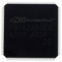
EZ80F91AZA50EG Zilog, EZ80F91AZA50EG Datasheet - Page 63

EZ80F91AZA50EG
Manufacturer Part Number
EZ80F91AZA50EG
Description
IC ACCLAIM MCU 256KB 144LQFP
Manufacturer
Zilog
Series
eZ80® AcclaimPlus!™r
Datasheet
1.EZ80F91AZA50SG.pdf
(387 pages)
Specifications of EZ80F91AZA50EG
Core Processor
Z8
Core Size
8-Bit
Speed
50MHz
Connectivity
Ethernet, I²C, IrDA, SPI, UART/USART
Peripherals
Brown-out Detect/Reset, POR, PWM, WDT
Number Of I /o
32
Program Memory Size
256KB (256K x 8)
Program Memory Type
FLASH
Ram Size
16K x 8
Voltage - Supply (vcc/vdd)
3 V ~ 3.6 V
Oscillator Type
Internal
Operating Temperature
-40°C ~ 105°C
Package / Case
144-LQFP
Processor Series
EZ80F91x
Core
eZ80
Data Bus Width
8 bit
Data Ram Size
16 KB
Interface Type
I2C, IrDA, SPI
Maximum Clock Frequency
50 MHz
Number Of Programmable I/os
32
Number Of Timers
4
Operating Supply Voltage
3 V to 3.6 V
Maximum Operating Temperature
+ 105 C
Mounting Style
SMD/SMT
Development Tools By Supplier
eZ80F910300ZCOG
Minimum Operating Temperature
- 40 C
For Use With
269-4712 - KIT DEV ENCORE 32 SERIES269-4671 - BOARD ZDOTS SBC Z80ACCLAIM PLUS269-4561 - KIT DEV FOR EZ80F91 W/C-COMPILER269-4560 - KIT DEV FOR EZ80F91 W/C-COMPILER
Lead Free Status / RoHS Status
Lead free / RoHS Compliant
Eeprom Size
-
Data Converters
-
Lead Free Status / Rohs Status
Details
Other names
269-4563
Available stocks
Company
Part Number
Manufacturer
Quantity
Price
- Current page: 63 of 387
- Download datasheet (5Mb)
Table 7. Port x Data Registers
(PA_DR = 0096h, PB_DR = 009Ah, PC_DR = 009Eh, PD_DR = 00A2h)
Table 8. Port x Data Direction Registers
(PA_DDR = 0097h, PB_DDR = 009Bh, PC_DDR = 009Fh, PD_DDR = 00A3h)
PS027001-0707
Bit
Reset
CPU Access
Note: X = Undefined; R/W = Read/Write.
Bit
Reset
CPU Access
Note: R/W = Read/Write.
GPIO Control Registers
Edge triggered interrupts are cleared by writing 1 to the corresponding bit of the Px_ALT0
register. For example, if PD4 has been set up to generate an edge triggered interrupt, the
interrupt is cleared by writing a 1 to Px_ALT0[4].
Each GPIO port has four registers that controls its operation. The operating mode of each
bit within a port is selected by writing to the corresponding bits of these four registers as
shown in
Data Direction register(Px_DDR), Port Alternate register 1(PX_ALT1), and Port Alternate
register 2(Px_ALT2). In addition to these four control registers, each port has a Port
Alternate register 0(Px_ALT0), which is used for clearing edge triggered interrupts.
Port x Data Registers
When the port pins are configured for one of the output modes, the data written to the
Port x Data registers (see
reading from the Port x Data registers always returns the sampled current value of the
corresponding pins. When the port pins are configured for edge triggered interrupts or
level-sensitive interrupts, the value written to the Port x Data register bit selects the
interrupt edge or interrupt level (for more details on GPIO mode selection, see
page 50).
Port x Data Direction Registers
In conjunction with the other GPIO Control registers, the Port x Data Direction registers
(see
mode selection, see
Table
Table 6
R/W
R/W
8) control the operating modes of the GPIO port pins. For more details on GPIO
X
7
7
1
on page 50. These four registers are Port Data register(Px_DR), Port
R/W
R/W
X
6
6
1
Table 6
Table
R/W
R/W
X
5
5
1
on page 50.
7) is driven on the corresponding pins. In all modes,
R/W
R/W
X
4
4
1
R/W
R/W
X
3
3
1
R/W
R/W
X
2
2
1
R/W
R/W
X
1
1
1
General Purpose Input/Output
Product Specification
R/W
R/W
X
0
0
1
eZ80F91 ASSP
Table 6
on
55
Related parts for EZ80F91AZA50EG
Image
Part Number
Description
Manufacturer
Datasheet
Request
R

Part Number:
Description:
Communication Controllers, ZILOG INTELLIGENT PERIPHERAL CONTROLLER (ZIP)
Manufacturer:
Zilog, Inc.
Datasheet:

Part Number:
Description:
KIT DEV FOR Z8 ENCORE 16K TO 64K
Manufacturer:
Zilog
Datasheet:

Part Number:
Description:
KIT DEV Z8 ENCORE XP 28-PIN
Manufacturer:
Zilog
Datasheet:

Part Number:
Description:
DEV KIT FOR Z8 ENCORE 8K/4K
Manufacturer:
Zilog
Datasheet:

Part Number:
Description:
KIT DEV Z8 ENCORE XP 28-PIN
Manufacturer:
Zilog
Datasheet:

Part Number:
Description:
DEV KIT FOR Z8 ENCORE 4K TO 8K
Manufacturer:
Zilog
Datasheet:

Part Number:
Description:
CMOS Z8 microcontroller. ROM 16 Kbytes, RAM 256 bytes, speed 16 MHz, 32 lines I/O, 3.0V to 5.5V
Manufacturer:
Zilog, Inc.
Datasheet:

Part Number:
Description:
Low-cost microcontroller. 512 bytes ROM, 61 bytes RAM, 8 MHz
Manufacturer:
Zilog, Inc.
Datasheet:

Part Number:
Description:
Z8 4K OTP Microcontroller
Manufacturer:
Zilog, Inc.
Datasheet:

Part Number:
Description:
CMOS SUPER8 ROMLESS MCU
Manufacturer:
Zilog, Inc.
Datasheet:

Part Number:
Description:
SL1866 CMOSZ8 OTP Microcontroller
Manufacturer:
Zilog, Inc.
Datasheet:

Part Number:
Description:
SL1866 CMOSZ8 OTP Microcontroller
Manufacturer:
Zilog, Inc.
Datasheet:

Part Number:
Description:
OTP (KB) = 1, RAM = 125, Speed = 12, I/O = 14, 8-bit Timers = 2, Comm Interfaces Other Features = Por, LV Protect, Voltage = 4.5-5.5V
Manufacturer:
Zilog, Inc.
Datasheet:

Part Number:
Description:
Manufacturer:
Zilog, Inc.
Datasheet:


