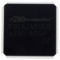
EZ80F91AZA50EG Zilog, EZ80F91AZA50EG Datasheet - Page 270

EZ80F91AZA50EG
Manufacturer Part Number
EZ80F91AZA50EG
Description
IC ACCLAIM MCU 256KB 144LQFP
Manufacturer
Zilog
Series
eZ80® AcclaimPlus!™r
Datasheet
1.EZ80F91AZA50SG.pdf
(387 pages)
Specifications of EZ80F91AZA50EG
Core Processor
Z8
Core Size
8-Bit
Speed
50MHz
Connectivity
Ethernet, I²C, IrDA, SPI, UART/USART
Peripherals
Brown-out Detect/Reset, POR, PWM, WDT
Number Of I /o
32
Program Memory Size
256KB (256K x 8)
Program Memory Type
FLASH
Ram Size
16K x 8
Voltage - Supply (vcc/vdd)
3 V ~ 3.6 V
Oscillator Type
Internal
Operating Temperature
-40°C ~ 105°C
Package / Case
144-LQFP
Processor Series
EZ80F91x
Core
eZ80
Data Bus Width
8 bit
Data Ram Size
16 KB
Interface Type
I2C, IrDA, SPI
Maximum Clock Frequency
50 MHz
Number Of Programmable I/os
32
Number Of Timers
4
Operating Supply Voltage
3 V to 3.6 V
Maximum Operating Temperature
+ 105 C
Mounting Style
SMD/SMT
Development Tools By Supplier
eZ80F910300ZCOG
Minimum Operating Temperature
- 40 C
For Use With
269-4712 - KIT DEV ENCORE 32 SERIES269-4671 - BOARD ZDOTS SBC Z80ACCLAIM PLUS269-4561 - KIT DEV FOR EZ80F91 W/C-COMPILER269-4560 - KIT DEV FOR EZ80F91 W/C-COMPILER
Lead Free Status / RoHS Status
Lead free / RoHS Compliant
Eeprom Size
-
Data Converters
-
Lead Free Status / Rohs Status
Details
Other names
269-4563
Available stocks
Company
Part Number
Manufacturer
Quantity
Price
- Current page: 270 of 387
- Download datasheet (5Mb)
Table 150. OCI Pins
PS027001-0707
Symbol
TCK
TRSTn
TMS
TDI
OCI Activation
OCI Interface
Name
Clock
TAP Reset
Test Mode Select
Data In
OCI features clock initialization circuitry so that external debug hardware is detected dur-
ing power-up. The external debugger must drive the OCI clock pin (TCK) Low at least
two system clock cycles prior to the end of the RESET to activate the OCI block. If TCK
is High at the end of the RESET, the OCI block shuts down so that it does not draw power
in normal product operation. When the OCI is shut down, ZDI is enabled directly and is
accessed via the clock (TCK) and data (TDI) pins. For more information on ZDI, see
Debug Interface
There are six dedicated pins on the eZ80F91 for the OCI interface. Four pins—TCK,
TMS, TDI, and TDO—are required for IEEE Standard 1149.1-compliant JTAG ports. A
fifth pin, TRSTn, is optional for IEEE 1149.1 and utilized by the eZ80F91 device. The
TRIGOUT pin provides additional testability features. These six OCI pins are described in
Table
150.
on page 235.
Type
Input
Input
Input
Input
(OCI enabled)
I/O
(OCI disabled)
Description
Asynchronous to the primary eZ80F91 system clock.
The TCK period must be at least twice the system
clock period. During RESET, this pin is sampled to
select either OCI or ZDI DEBUG modes. If Low
during RESET, the OCI is enabled. If High during
RESET, the OCI is powered down and ZDI DEBUG
mode is enabled. When ZDI DEBUG mode is active,
this pin is the ZDI clock. On-chip pull-up ensures a
default value of 1 (High).
Active Low asynchronous reset for the Test Access
Port state register. On-chip pull-up ensures a default
value of 1 (High).
This serial test mode input controls JTAG mode
selection. On-chip pull-up ensures a default value of
1 (High). The TMS signal is sampled on the rising
edge of the TCK signal.
Serial test data input. This pin is input-only when the
OCI is enabled. The input data is sampled on the
rising edge of the TCK signal.
When the OCI is disabled, this pin functions as the
ZDA (ZDI Data) I/O pin. NORMAL mode, following
RESET, configures TDI as an input.
Product Specification
On-Chip Instrumentation
eZ80F91 ASSP
Zilog
262
Related parts for EZ80F91AZA50EG
Image
Part Number
Description
Manufacturer
Datasheet
Request
R

Part Number:
Description:
Communication Controllers, ZILOG INTELLIGENT PERIPHERAL CONTROLLER (ZIP)
Manufacturer:
Zilog, Inc.
Datasheet:

Part Number:
Description:
KIT DEV FOR Z8 ENCORE 16K TO 64K
Manufacturer:
Zilog
Datasheet:

Part Number:
Description:
KIT DEV Z8 ENCORE XP 28-PIN
Manufacturer:
Zilog
Datasheet:

Part Number:
Description:
DEV KIT FOR Z8 ENCORE 8K/4K
Manufacturer:
Zilog
Datasheet:

Part Number:
Description:
KIT DEV Z8 ENCORE XP 28-PIN
Manufacturer:
Zilog
Datasheet:

Part Number:
Description:
DEV KIT FOR Z8 ENCORE 4K TO 8K
Manufacturer:
Zilog
Datasheet:

Part Number:
Description:
CMOS Z8 microcontroller. ROM 16 Kbytes, RAM 256 bytes, speed 16 MHz, 32 lines I/O, 3.0V to 5.5V
Manufacturer:
Zilog, Inc.
Datasheet:

Part Number:
Description:
Low-cost microcontroller. 512 bytes ROM, 61 bytes RAM, 8 MHz
Manufacturer:
Zilog, Inc.
Datasheet:

Part Number:
Description:
Z8 4K OTP Microcontroller
Manufacturer:
Zilog, Inc.
Datasheet:

Part Number:
Description:
CMOS SUPER8 ROMLESS MCU
Manufacturer:
Zilog, Inc.
Datasheet:

Part Number:
Description:
SL1866 CMOSZ8 OTP Microcontroller
Manufacturer:
Zilog, Inc.
Datasheet:

Part Number:
Description:
SL1866 CMOSZ8 OTP Microcontroller
Manufacturer:
Zilog, Inc.
Datasheet:

Part Number:
Description:
OTP (KB) = 1, RAM = 125, Speed = 12, I/O = 14, 8-bit Timers = 2, Comm Interfaces Other Features = Por, LV Protect, Voltage = 4.5-5.5V
Manufacturer:
Zilog, Inc.
Datasheet:

Part Number:
Description:
Manufacturer:
Zilog, Inc.
Datasheet:


