HD64F38024DV Renesas Electronics America, HD64F38024DV Datasheet - Page 11
HD64F38024DV
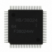
Manufacturer Part Number
HD64F38024DV
Description
IC H8/SLP MCU FLASH 80QFP
Manufacturer
Renesas Electronics America
Series
H8® H8/300L SLPr
Datasheets
1.US38024-BAG1.pdf
(684 pages)
2.DF36012GFYV.pdf
(1021 pages)
3.DF38102HV.pdf
(145 pages)
Specifications of HD64F38024DV
Core Processor
H8/300L
Core Size
8-Bit
Speed
10MHz
Connectivity
SCI
Peripherals
LCD, PWM, WDT
Number Of I /o
51
Program Memory Size
32KB (32K x 8)
Program Memory Type
FLASH
Ram Size
1K x 8
Voltage - Supply (vcc/vdd)
1.8 V ~ 5.5 V
Data Converters
A/D 8x10b
Oscillator Type
Internal
Operating Temperature
-40°C ~ 85°C
Package / Case
80-QFP
Lead Free Status / RoHS Status
Lead free / RoHS Compliant
Eeprom Size
-
Available stocks
Company
Part Number
Manufacturer
Quantity
Price
Company:

Part Number:
HD64F38024DV
Manufacturer:
Renesas Electronics America
Quantity:
10 000


Section 1 Overview................................................................................................1
1.1
1.2
1.3
Section 2 CPU......................................................................................................25
2.1
2.2
2.3
2.4
2.5
2.6
2.7
Overview................................................................................................................................ 1
Internal Block Diagram.......................................................................................................... 7
Pin Arrangement and Functions............................................................................................. 9
1.3.1
1.3.2
Overview.............................................................................................................................. 25
2.1.1
2.1.2
2.1.3
Register Descriptions ........................................................................................................... 27
2.2.1
2.2.2
2.2.3
Data Formats ........................................................................................................................ 29
2.3.1
2.3.2
Addressing Modes................................................................................................................ 32
2.4.1
2.4.2
Instruction Set ...................................................................................................................... 38
2.5.1
2.5.2
2.5.3
2.5.4
2.5.5
2.5.6
2.5.7
2.5.8
Basic Operational Timing .................................................................................................... 55
2.6.1
2.6.2
CPU States ........................................................................................................................... 57
2.7.1
2.7.2
Pin Arrangement ....................................................................................................... 9
Pin Functions .......................................................................................................... 19
Features................................................................................................................... 25
Address Space......................................................................................................... 26
Register Configuration............................................................................................ 26
General Registers .................................................................................................... 27
Control Registers .................................................................................................... 27
Initial Register Values............................................................................................. 29
Data Formats in General Registers ......................................................................... 30
Memory Data Formats ............................................................................................ 31
Addressing Modes .................................................................................................. 32
Effective Address Calculation ................................................................................ 34
Data Transfer Instructions....................................................................................... 40
Arithmetic Operations............................................................................................. 42
Logic Operations..................................................................................................... 43
Shift Operations ...................................................................................................... 44
Bit Manipulations.................................................................................................... 46
Branching Instructions ............................................................................................ 50
System Control Instructions.................................................................................... 52
Block Data Transfer Instruction.............................................................................. 53
Access to On-Chip Memory (RAM, ROM)............................................................ 55
Access to On-Chip Peripheral Modules .................................................................. 56
Overview................................................................................................................. 57
Program Execution State......................................................................................... 59
Contents
Rev. 8.00 Mar. 09, 2010 Page ix of xx
REJ09B0042-0800
Related parts for HD64F38024DV
Image
Part Number
Description
Manufacturer
Datasheet
Request
R


Part Number:
Description:
KIT STARTER FOR M16C/29
Manufacturer:
Renesas Electronics America
Datasheet:

Part Number:
Description:
KIT STARTER FOR R8C/2D
Manufacturer:
Renesas Electronics America
Datasheet:

Part Number:
Description:
R0K33062P STARTER KIT
Manufacturer:
Renesas Electronics America
Datasheet:

Part Number:
Description:
KIT STARTER FOR R8C/23 E8A
Manufacturer:
Renesas Electronics America
Datasheet:

Part Number:
Description:
KIT STARTER FOR R8C/25
Manufacturer:
Renesas Electronics America
Datasheet:

Part Number:
Description:
KIT STARTER H8S2456 SHARPE DSPLY
Manufacturer:
Renesas Electronics America
Datasheet:

Part Number:
Description:
KIT STARTER FOR R8C38C
Manufacturer:
Renesas Electronics America
Datasheet:

Part Number:
Description:
KIT STARTER FOR R8C35C
Manufacturer:
Renesas Electronics America
Datasheet:

Part Number:
Description:
KIT STARTER FOR R8CL3AC+LCD APPS
Manufacturer:
Renesas Electronics America
Datasheet:
Part Number:
Description:
KIT STARTER FOR RX610
Manufacturer:
Renesas Electronics America
Datasheet:

Part Number:
Description:
KIT STARTER FOR R32C/118
Manufacturer:
Renesas Electronics America
Datasheet:

Part Number:
Description:
KIT DEV RSK-R8C/26-29
Manufacturer:
Renesas Electronics America
Datasheet:

Part Number:
Description:
KIT STARTER FOR SH7124
Manufacturer:
Renesas Electronics America
Datasheet:

Part Number:
Description:
KIT STARTER FOR H8SX/1622
Manufacturer:
Renesas Electronics America
Datasheet: