HD64F38024DV Renesas Electronics America, HD64F38024DV Datasheet - Page 192
HD64F38024DV
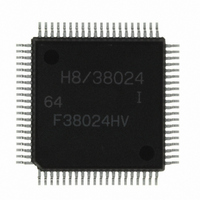
Manufacturer Part Number
HD64F38024DV
Description
IC H8/SLP MCU FLASH 80QFP
Manufacturer
Renesas Electronics America
Series
H8® H8/300L SLPr
Datasheets
1.US38024-BAG1.pdf
(684 pages)
2.DF36012GFYV.pdf
(1021 pages)
3.DF38102HV.pdf
(145 pages)
Specifications of HD64F38024DV
Core Processor
H8/300L
Core Size
8-Bit
Speed
10MHz
Connectivity
SCI
Peripherals
LCD, PWM, WDT
Number Of I /o
51
Program Memory Size
32KB (32K x 8)
Program Memory Type
FLASH
Ram Size
1K x 8
Voltage - Supply (vcc/vdd)
1.8 V ~ 5.5 V
Data Converters
A/D 8x10b
Oscillator Type
Internal
Operating Temperature
-40°C ~ 85°C
Package / Case
80-QFP
Lead Free Status / RoHS Status
Lead free / RoHS Compliant
Eeprom Size
-
Available stocks
Company
Part Number
Manufacturer
Quantity
Price
Company:

Part Number:
HD64F38024DV
Manufacturer:
Renesas Electronics America
Quantity:
10 000


Section 6 ROM
6.7.3
1. You must use the system clock oscillator when programming or erasing flash memory on the
2. On the H8/38124 Group the watchdog timer operates after a reset is canceled. When executing
6.8
A software method using the CPU is employed to program and erase flash memory in the on-
board programming modes. Depending on the FLMCR1 setting, the flash memory operates in one
of the following four modes: Program mode, program-verify mode, erase mode, and erase-verify
mode. The programming control program in boot mode and the user program/erase control
program in user program mode use these operating modes in combination to perform
programming/erasing. Flash memory programming and erasing should be performed in
accordance with the descriptions in section 6.8.1, Program/Program-Verify and section 6.8.2,
Erase/Erase-Verify, respectively.
6.8.1
When writing data or programs to the flash memory, the program/program-verify flowchart shown
in figure 6.10 should be followed. Performing programming operations according to this
flowchart will enable data or programs to be written to the flash memory without subjecting the
chip to voltage stress or sacrificing program data reliability.
1. Programming must be done to an empty address. Do not reprogram an address to which
2. Programming should be carried out 128 bytes at a time. A 128-byte data transfer must be
3. Prepare the following data storage areas in RAM: A 128-byte programming data area, a 128-
Rev. 8.00 Mar. 09, 2010 Page 170 of 658
REJ09B0042-0800
H8/38124 Group. The on-chip oscillator should not be used for programming or erasing flash
memory. See section 4.2, On-Chip Oscillator Selection Method, for information on switching
between the system clock oscillator and the on-chip oscillator.
a program prepared by the user that performs programming and erasing in the user mode, the
watchdog timer’s overflow cycle should be set to an appropriate value. Refer to section 6.8.1,
Program/Program-Verify, for information on the appropriate watchdog timer overflow cycle
for programming, and refer to section 6.8.2, Erase/Erase-Verify, for information on the
appropriate watchdog timer overflow cycle for erasing.
programming has already been performed.
performed even if writing fewer than 128 bytes. In this case, H'FF data must be written to the
extra addresses.
byte reprogramming data area, and a 128-byte additional-programming data area. Perform
Notes on On-Board Programming
Flash Memory Programming/Erasing
Program/Program-Verify
Related parts for HD64F38024DV
Image
Part Number
Description
Manufacturer
Datasheet
Request
R


Part Number:
Description:
KIT STARTER FOR M16C/29
Manufacturer:
Renesas Electronics America
Datasheet:

Part Number:
Description:
KIT STARTER FOR R8C/2D
Manufacturer:
Renesas Electronics America
Datasheet:

Part Number:
Description:
R0K33062P STARTER KIT
Manufacturer:
Renesas Electronics America
Datasheet:

Part Number:
Description:
KIT STARTER FOR R8C/23 E8A
Manufacturer:
Renesas Electronics America
Datasheet:

Part Number:
Description:
KIT STARTER FOR R8C/25
Manufacturer:
Renesas Electronics America
Datasheet:

Part Number:
Description:
KIT STARTER H8S2456 SHARPE DSPLY
Manufacturer:
Renesas Electronics America
Datasheet:

Part Number:
Description:
KIT STARTER FOR R8C38C
Manufacturer:
Renesas Electronics America
Datasheet:

Part Number:
Description:
KIT STARTER FOR R8C35C
Manufacturer:
Renesas Electronics America
Datasheet:

Part Number:
Description:
KIT STARTER FOR R8CL3AC+LCD APPS
Manufacturer:
Renesas Electronics America
Datasheet:
Part Number:
Description:
KIT STARTER FOR RX610
Manufacturer:
Renesas Electronics America
Datasheet:

Part Number:
Description:
KIT STARTER FOR R32C/118
Manufacturer:
Renesas Electronics America
Datasheet:

Part Number:
Description:
KIT DEV RSK-R8C/26-29
Manufacturer:
Renesas Electronics America
Datasheet:

Part Number:
Description:
KIT STARTER FOR SH7124
Manufacturer:
Renesas Electronics America
Datasheet:

Part Number:
Description:
KIT STARTER FOR H8SX/1622
Manufacturer:
Renesas Electronics America
Datasheet: