HD64F38024DV Renesas Electronics America, HD64F38024DV Datasheet - Page 312
HD64F38024DV
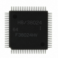
Manufacturer Part Number
HD64F38024DV
Description
IC H8/SLP MCU FLASH 80QFP
Manufacturer
Renesas Electronics America
Series
H8® H8/300L SLPr
Datasheets
1.US38024-BAG1.pdf
(684 pages)
2.DF36012GFYV.pdf
(1021 pages)
3.DF38102HV.pdf
(145 pages)
Specifications of HD64F38024DV
Core Processor
H8/300L
Core Size
8-Bit
Speed
10MHz
Connectivity
SCI
Peripherals
LCD, PWM, WDT
Number Of I /o
51
Program Memory Size
32KB (32K x 8)
Program Memory Type
FLASH
Ram Size
1K x 8
Voltage - Supply (vcc/vdd)
1.8 V ~ 5.5 V
Data Converters
A/D 8x10b
Oscillator Type
Internal
Operating Temperature
-40°C ~ 85°C
Package / Case
80-QFP
Lead Free Status / RoHS Status
Lead free / RoHS Compliant
Eeprom Size
-
Available stocks
Company
Part Number
Manufacturer
Quantity
Price
Company:

Part Number:
HD64F38024DV
Manufacturer:
Renesas Electronics America
Quantity:
10 000


Section 9 Timers
9.5.3
The noise canceler consists of a digital low-pass filter that eliminates high-frequency component
noise from the pulses input from the input capture input pin. The noise canceler is set by NCS * in
PMR2.
Figure 9.9 shows a block diagram of the noise canceler.
The noise canceler consists of five latch circuits connected in series and a match detector circuit.
When the noise cancellation function is not used (NCS = 0), the system clock is selected as the
sampling clock. When the noise cancellation function is used (NCS = 1), the sampling clock is the
internal clock selected by CKS1 and CKS0 in TMG, the input capture input is sampled on the
rising edge of this clock, and the data is judged to be correct when all the latch outputs match. If
all the outputs do not match, the previous value is retained. After a reset, the noise canceler output
is initialized when the falling edge of the input capture input signal has been sampled five times.
Therefore, after making a setting for use of the noise cancellation function, a pulse with at least
five times the width of the sampling clock is a dependable input capture signal. Even if noise
cancellation is not used, an input capture input signal pulse width of at least 2φ or 2φ
necessary to ensure that input capture operations are performed properly
Note: * An input capture signal may be generated when the NCS bit is modified.
Figure 9.10 shows an example of noise canceler timing.
Rev. 8.00 Mar. 09, 2010 Page 290 of 658
REJ09B0042-0800
Input capture
input signal
Sampling clock
Noise Canceler
Sampling
D
clock
Latch
C
Δt: Set by CKS1 and CKS0
Q
Δt
D
Figure 9.9 Noise Canceler Block Diagram
Latch
C
Q
D
Latch
C
Q
D
Latch
C
Q
D
Latch
C
Q
detector
Match
SUB
is
Noise
canceler
output
Related parts for HD64F38024DV
Image
Part Number
Description
Manufacturer
Datasheet
Request
R


Part Number:
Description:
KIT STARTER FOR M16C/29
Manufacturer:
Renesas Electronics America
Datasheet:

Part Number:
Description:
KIT STARTER FOR R8C/2D
Manufacturer:
Renesas Electronics America
Datasheet:

Part Number:
Description:
R0K33062P STARTER KIT
Manufacturer:
Renesas Electronics America
Datasheet:

Part Number:
Description:
KIT STARTER FOR R8C/23 E8A
Manufacturer:
Renesas Electronics America
Datasheet:

Part Number:
Description:
KIT STARTER FOR R8C/25
Manufacturer:
Renesas Electronics America
Datasheet:

Part Number:
Description:
KIT STARTER H8S2456 SHARPE DSPLY
Manufacturer:
Renesas Electronics America
Datasheet:

Part Number:
Description:
KIT STARTER FOR R8C38C
Manufacturer:
Renesas Electronics America
Datasheet:

Part Number:
Description:
KIT STARTER FOR R8C35C
Manufacturer:
Renesas Electronics America
Datasheet:

Part Number:
Description:
KIT STARTER FOR R8CL3AC+LCD APPS
Manufacturer:
Renesas Electronics America
Datasheet:
Part Number:
Description:
KIT STARTER FOR RX610
Manufacturer:
Renesas Electronics America
Datasheet:

Part Number:
Description:
KIT STARTER FOR R32C/118
Manufacturer:
Renesas Electronics America
Datasheet:

Part Number:
Description:
KIT DEV RSK-R8C/26-29
Manufacturer:
Renesas Electronics America
Datasheet:

Part Number:
Description:
KIT STARTER FOR SH7124
Manufacturer:
Renesas Electronics America
Datasheet:

Part Number:
Description:
KIT STARTER FOR H8SX/1622
Manufacturer:
Renesas Electronics America
Datasheet: