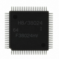
HD64F38024DV Renesas Electronics America, HD64F38024DV Datasheet - Page 254

HD64F38024DV
Manufacturer Part Number
HD64F38024DV
Description
IC H8/SLP MCU FLASH 80QFP
Manufacturer
Renesas Electronics America
Series
H8® H8/300L SLPr
Datasheets
1.US38024-BAG1.pdf
(684 pages)
2.DF36012GFYV.pdf
(1021 pages)
3.DF38102HV.pdf
(145 pages)
Specifications of HD64F38024DV
Core Processor
H8/300L
Core Size
8-Bit
Speed
10MHz
Connectivity
SCI
Peripherals
LCD, PWM, WDT
Number Of I /o
51
Program Memory Size
32KB (32K x 8)
Program Memory Type
FLASH
Ram Size
1K x 8
Voltage - Supply (vcc/vdd)
1.8 V ~ 5.5 V
Data Converters
A/D 8x10b
Oscillator Type
Internal
Operating Temperature
-40°C ~ 85°C
Package / Case
80-QFP
Lead Free Status / RoHS Status
Lead free / RoHS Compliant
Eeprom Size
-
Available stocks
Company
Part Number
Manufacturer
Quantity
Price
Company:
Part Number:
HD64F38024DV
Manufacturer:
Renesas Electronics America
Quantity:
10 000
- Current page: 254 of 684
- Download datasheet (5Mb)
Section 8 I/O Ports
Bit 3— P9
Bit 3 turns the P9
and H8/38124 Group.
Bit 3
PIOFF
0
1
Note: In the H8/38024 ZTAT version and mask ROM version, and the HD64F38024R, the
Rev. 8.00 Mar. 09, 2010 Page 232 of 658
REJ09B0042-0800
following precautions should be followed when accessing the PIOFF bit.
When turning the voltage boost circuit on or off, always write to the register when the buffer
NMOS is off (port data set to 1). Also, when turning on the voltage boost circuit, first clear
PIOFF to 0 and then after waiting 30 system clock cycles turn on the buffer NMOS (port
data cleared to 0). If 30 system clock cycles have not elapsed the voltage boost circuit will
not start operating and it will not be possible to produce a large current flow, resulting in
unstable operation.
In the HD64F38024, the following precautions should be followed when accessing the
PIOFF bit.
In the HD64F38024, if port data bits are cleared from 1 to 0 while the PIOFF bit is set to 1,
repeated charge-discharge cycles will occur in the voltage boost circuit, causing the current
consumption to rise and fall cyclically. The amount of rise in the current consumption in this
case is between several tens of µA and 100 µA above the normal level. Therefore, the
following points should be kept in mind.
(1) Not Using Subclock
(2) Not Using Port 9
(3) Using Port 9 with PIOFF Always Cleared to 0
(4) Using Port 9 with PIOFF Set to 1
2
Regardless of whether or not port 9 is used, the PIOFF bit should be left at its initial
value (0) and not changed.
Port data should be used unchanged with the PIOFF bit either at its initial value (0) or
set to 1. In the latter case the current consumption will vary, due to the intermittent
operation of the voltage boost circuit, by about 1 µA (standby mode or watch mode, V
= 3.0 V, Ta = 25°C).
This case applies to instances in which the voltage boost circuit is used constantly to
generate a large current glow, or an increase in current consumption due to the
operation of the voltage boost circuit is permissible even in the standby mode or watch
mode (see (2) above). In this case the PIOFF bit should be left at its initial value (0) and
not changed.
This case applies to instances in which it is necessary to change the value of the PIOFF
bit due to operating conditions or where it is desirable to keep the PIOFF bit set to 1
because no large current is required (for example, shutting down the voltage boost
circuit to reduce current consumption in the watch mode). In this case, clear port data
to P9
Description
Large-current port step-up circuit is turned on
Large-current port step-up circuit is turned off
2
0
to P9
Step-Up Circuit Control (PIOFF)
0
step-up circuit on and off. This bit is reserved in the H8/38024S Group
(initial value)
CC
Related parts for HD64F38024DV
Image
Part Number
Description
Manufacturer
Datasheet
Request
R

Part Number:
Description:
KIT STARTER FOR M16C/29
Manufacturer:
Renesas Electronics America
Datasheet:

Part Number:
Description:
KIT STARTER FOR R8C/2D
Manufacturer:
Renesas Electronics America
Datasheet:

Part Number:
Description:
R0K33062P STARTER KIT
Manufacturer:
Renesas Electronics America
Datasheet:

Part Number:
Description:
KIT STARTER FOR R8C/23 E8A
Manufacturer:
Renesas Electronics America
Datasheet:

Part Number:
Description:
KIT STARTER FOR R8C/25
Manufacturer:
Renesas Electronics America
Datasheet:

Part Number:
Description:
KIT STARTER H8S2456 SHARPE DSPLY
Manufacturer:
Renesas Electronics America
Datasheet:

Part Number:
Description:
KIT STARTER FOR R8C38C
Manufacturer:
Renesas Electronics America
Datasheet:

Part Number:
Description:
KIT STARTER FOR R8C35C
Manufacturer:
Renesas Electronics America
Datasheet:

Part Number:
Description:
KIT STARTER FOR R8CL3AC+LCD APPS
Manufacturer:
Renesas Electronics America
Datasheet:

Part Number:
Description:
KIT STARTER FOR RX610
Manufacturer:
Renesas Electronics America
Datasheet:

Part Number:
Description:
KIT STARTER FOR R32C/118
Manufacturer:
Renesas Electronics America
Datasheet:

Part Number:
Description:
KIT DEV RSK-R8C/26-29
Manufacturer:
Renesas Electronics America
Datasheet:

Part Number:
Description:
KIT STARTER FOR SH7124
Manufacturer:
Renesas Electronics America
Datasheet:

Part Number:
Description:
KIT STARTER FOR H8SX/1622
Manufacturer:
Renesas Electronics America
Datasheet:


