HD64F38024DV Renesas Electronics America, HD64F38024DV Datasheet - Page 92
HD64F38024DV
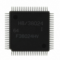
Manufacturer Part Number
HD64F38024DV
Description
IC H8/SLP MCU FLASH 80QFP
Manufacturer
Renesas Electronics America
Series
H8® H8/300L SLPr
Datasheets
1.US38024-BAG1.pdf
(684 pages)
2.DF36012GFYV.pdf
(1021 pages)
3.DF38102HV.pdf
(145 pages)
Specifications of HD64F38024DV
Core Processor
H8/300L
Core Size
8-Bit
Speed
10MHz
Connectivity
SCI
Peripherals
LCD, PWM, WDT
Number Of I /o
51
Program Memory Size
32KB (32K x 8)
Program Memory Type
FLASH
Ram Size
1K x 8
Voltage - Supply (vcc/vdd)
1.8 V ~ 5.5 V
Data Converters
A/D 8x10b
Oscillator Type
Internal
Operating Temperature
-40°C ~ 85°C
Package / Case
80-QFP
Lead Free Status / RoHS Status
Lead free / RoHS Compliant
Eeprom Size
-
Available stocks
Company
Part Number
Manufacturer
Quantity
Price
Company:

Part Number:
HD64F38024DV
Manufacturer:
Renesas Electronics America
Quantity:
10 000


Section 2 CPU
To avoid this problem, store a copy of the PDR3 data in a work area in memory. Perform the bit
manipulation on the data in the work area, then write this data to PDR3.
[A: Prior to executing BSET]
Input/output Input
Pin state
PCR3
PDR3
RAM0
[B: BSET instruction executed]
[C: After executing BSET]
Input/output Input
Pin state
PCR3
PDR3
RAM0
Rev. 8.00 Mar. 09, 2010 Page 70 of 658
REJ09B0042-0800
MOV. B
MOV. B
MOV. B
BSET
MOV. B
MOV. B
#0
#80,
R0L,
R0L,
@RAM0, R0L
R0L,
P3
Low level High level Low level Low level Low level Low level Low level Low level
0
1
1
P3
Low level High level Low level Low level Low level Low level Low level High level
0
1
1
7
7
,
@RAM0
R0L
@RAM0
@PDR3
@PDR3
P3
Input
0
0
0
P3
Input
0
0
0
6
6
P3
Output
1
0
0
P3
Output
1
0
0
The PDR3 value (H'80) is written to a work area in memory
(RAM0) as well as to PDR3
The BSET instruction is executed designating the PDR3
work area (RAM0).
The work area (RAM0) value is written to PDR3.
5
5
P3
Output
1
0
0
P3
Output
1
0
0
4
4
P3
Output
1
0
0
P3
Output
1
0
0
3
3
P3
Output
1
0
0
P3
Output
1
0
0
2
2
P3
Output
1
0
0
P3
Output
1
0
0
1
1
P3
Output
1
0
0
P3
Output
1
1
1
0
0
Related parts for HD64F38024DV
Image
Part Number
Description
Manufacturer
Datasheet
Request
R


Part Number:
Description:
KIT STARTER FOR M16C/29
Manufacturer:
Renesas Electronics America
Datasheet:

Part Number:
Description:
KIT STARTER FOR R8C/2D
Manufacturer:
Renesas Electronics America
Datasheet:

Part Number:
Description:
R0K33062P STARTER KIT
Manufacturer:
Renesas Electronics America
Datasheet:

Part Number:
Description:
KIT STARTER FOR R8C/23 E8A
Manufacturer:
Renesas Electronics America
Datasheet:

Part Number:
Description:
KIT STARTER FOR R8C/25
Manufacturer:
Renesas Electronics America
Datasheet:

Part Number:
Description:
KIT STARTER H8S2456 SHARPE DSPLY
Manufacturer:
Renesas Electronics America
Datasheet:

Part Number:
Description:
KIT STARTER FOR R8C38C
Manufacturer:
Renesas Electronics America
Datasheet:

Part Number:
Description:
KIT STARTER FOR R8C35C
Manufacturer:
Renesas Electronics America
Datasheet:

Part Number:
Description:
KIT STARTER FOR R8CL3AC+LCD APPS
Manufacturer:
Renesas Electronics America
Datasheet:
Part Number:
Description:
KIT STARTER FOR RX610
Manufacturer:
Renesas Electronics America
Datasheet:

Part Number:
Description:
KIT STARTER FOR R32C/118
Manufacturer:
Renesas Electronics America
Datasheet:

Part Number:
Description:
KIT DEV RSK-R8C/26-29
Manufacturer:
Renesas Electronics America
Datasheet:

Part Number:
Description:
KIT STARTER FOR SH7124
Manufacturer:
Renesas Electronics America
Datasheet:

Part Number:
Description:
KIT STARTER FOR H8SX/1622
Manufacturer:
Renesas Electronics America
Datasheet: