HD64F38024DV Renesas Electronics America, HD64F38024DV Datasheet - Page 406
HD64F38024DV
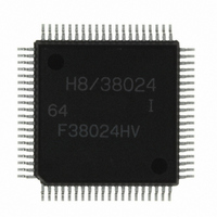
Manufacturer Part Number
HD64F38024DV
Description
IC H8/SLP MCU FLASH 80QFP
Manufacturer
Renesas Electronics America
Series
H8® H8/300L SLPr
Datasheets
1.US38024-BAG1.pdf
(684 pages)
2.DF36012GFYV.pdf
(1021 pages)
3.DF38102HV.pdf
(145 pages)
Specifications of HD64F38024DV
Core Processor
H8/300L
Core Size
8-Bit
Speed
10MHz
Connectivity
SCI
Peripherals
LCD, PWM, WDT
Number Of I /o
51
Program Memory Size
32KB (32K x 8)
Program Memory Type
FLASH
Ram Size
1K x 8
Voltage - Supply (vcc/vdd)
1.8 V ~ 5.5 V
Data Converters
A/D 8x10b
Oscillator Type
Internal
Operating Temperature
-40°C ~ 85°C
Package / Case
80-QFP
Lead Free Status / RoHS Status
Lead free / RoHS Compliant
Eeprom Size
-
Available stocks
Company
Part Number
Manufacturer
Quantity
Price
Company:

Part Number:
HD64F38024DV
Manufacturer:
Renesas Electronics America
Quantity:
10 000


Section 10 Serial Communication Interface
8. Transmit and receive operations when making a state transition
Make sure that transmit and receive operations have completely finished before carrying out state
transition processing.
9. Switching SCK
If pin SCK
general input/output pin (a pin with a different function), the pin outputs a low level signal for half
a system clock (φ) cycle immediately after it is switched.
This can be prevented by either of the following methods according to the situation.
a. When an SCK
b. When an SCK
10. Set up at subactive or subsleep mode
At subactive or subsleep mode, SCI3 becomes possible use only at CPU clock is φw/2.
11. Oscillator use with serial communications interface (H8/38124 Group only)
When implementing the serial communications interface on the H8/38124 Group, the system
clock oscillator must be used. The on-chip oscillator should not be used in this case. See on-chip
oscillator selection method in section 4.2, System Clock Generator, for information on switching
between the system clock oscillator and the on-chip oscillator.
Rev. 8.00 Mar. 09, 2010 Page 384 of 658
REJ09B0042-0800
When stopping data transfer, issue one instruction to clear bits TE and RE to 0 and to set bits
CKE1 and CKE0 in SCR3 to 1 and 0, respectively. In this case, bit COM in SMR should be
left 1. The above prevents SCK
intermediate level of voltage from being applied to SCK
be pulled up to the V
When stopping data transfer,
(i) Issue one instruction to clear bits TE and RE to 0 and to set bits CKE1 and CKE0 in SCR3
(ii) Clear bit COM in SMR to 0
(iii) Clear bits CKE1 and CKE0 in SCR3 to 0
Note that special care is also needed here to avoid an intermediate level of voltage from being
applied to SCK
to 1 and 0, respectively.
32
is used as a clock output pin by SCI3 in synchronous mode and is then switched to a
32
32
32
32
function is switched from clock output to non clock-output
function is switched from clock output to general input/output
.
function
CC
level via a resistor, or supplied with output from an external device.
32
from being used as a general input/output pin. To avoid an
32
, the line connected to SCK
32
should
Related parts for HD64F38024DV
Image
Part Number
Description
Manufacturer
Datasheet
Request
R


Part Number:
Description:
KIT STARTER FOR M16C/29
Manufacturer:
Renesas Electronics America
Datasheet:

Part Number:
Description:
KIT STARTER FOR R8C/2D
Manufacturer:
Renesas Electronics America
Datasheet:

Part Number:
Description:
R0K33062P STARTER KIT
Manufacturer:
Renesas Electronics America
Datasheet:

Part Number:
Description:
KIT STARTER FOR R8C/23 E8A
Manufacturer:
Renesas Electronics America
Datasheet:

Part Number:
Description:
KIT STARTER FOR R8C/25
Manufacturer:
Renesas Electronics America
Datasheet:

Part Number:
Description:
KIT STARTER H8S2456 SHARPE DSPLY
Manufacturer:
Renesas Electronics America
Datasheet:

Part Number:
Description:
KIT STARTER FOR R8C38C
Manufacturer:
Renesas Electronics America
Datasheet:

Part Number:
Description:
KIT STARTER FOR R8C35C
Manufacturer:
Renesas Electronics America
Datasheet:

Part Number:
Description:
KIT STARTER FOR R8CL3AC+LCD APPS
Manufacturer:
Renesas Electronics America
Datasheet:
Part Number:
Description:
KIT STARTER FOR RX610
Manufacturer:
Renesas Electronics America
Datasheet:

Part Number:
Description:
KIT STARTER FOR R32C/118
Manufacturer:
Renesas Electronics America
Datasheet:

Part Number:
Description:
KIT DEV RSK-R8C/26-29
Manufacturer:
Renesas Electronics America
Datasheet:

Part Number:
Description:
KIT STARTER FOR SH7124
Manufacturer:
Renesas Electronics America
Datasheet:

Part Number:
Description:
KIT STARTER FOR H8SX/1622
Manufacturer:
Renesas Electronics America
Datasheet: