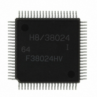
HD64F38024DV Renesas Electronics America, HD64F38024DV Datasheet - Page 396

HD64F38024DV
Manufacturer Part Number
HD64F38024DV
Description
IC H8/SLP MCU FLASH 80QFP
Manufacturer
Renesas Electronics America
Series
H8® H8/300L SLPr
Datasheets
1.US38024-BAG1.pdf
(684 pages)
2.DF36012GFYV.pdf
(1021 pages)
3.DF38102HV.pdf
(145 pages)
Specifications of HD64F38024DV
Core Processor
H8/300L
Core Size
8-Bit
Speed
10MHz
Connectivity
SCI
Peripherals
LCD, PWM, WDT
Number Of I /o
51
Program Memory Size
32KB (32K x 8)
Program Memory Type
FLASH
Ram Size
1K x 8
Voltage - Supply (vcc/vdd)
1.8 V ~ 5.5 V
Data Converters
A/D 8x10b
Oscillator Type
Internal
Operating Temperature
-40°C ~ 85°C
Package / Case
80-QFP
Lead Free Status / RoHS Status
Lead free / RoHS Compliant
Eeprom Size
-
Available stocks
Company
Part Number
Manufacturer
Quantity
Price
Company:
Part Number:
HD64F38024DV
Manufacturer:
Renesas Electronics America
Quantity:
10 000
- Current page: 396 of 684
- Download datasheet (5Mb)
Section 10 Serial Communication Interface
SCI3 operates as follows when transmitting data.
SCI3 monitors bit TDRE in SSR, and when it is cleared to 0, recognizes that data has been written
to TDR and transfers data from TDR to TSR. It then sets bit TDRE to 1 and starts transmitting. If
bit TIE in SCR3 is set to 1 at this time, a TXI request is made.
When clock output mode is selected, SCI3 outputs 8 serial clock pulses. When an external clock
is selected, data is output in synchronization with the input clock.
Serial data is transmitted from the TXD32 pin in order from the LSB (bit 0) to the MSB (bit 7).
When the MSB (bit 7) is sent, checks bit TDRE. If bit TDRE is cleared to 0, SCI3 transfers data
from TDR to TSR, and starts transmission of the next frame. If bit TDRE is set to 1, SCI3 sets bit
TEND to 1 in SSR, and after sending the MSB (bit 7), retains the MSB state. If bit TEIE in SCR3
is set to 1 at this time, a TEI request is made.
After transmission ends, the SCK pin is fixed at the high level.
Note: Transmission is not possible if an error flag (OER, FER, or PER) that indicates the data
Figure 10.12 shows an example of the operation when transmitting in synchronous mode.
Rev. 8.00 Mar. 09, 2010 Page 374 of 658
REJ09B0042-0800
TDRE
TEND
LSI
operation
User
processing
Serial
clock
Serial
data
Figure 10.12 Example of Operation when Transmitting in Synchronous Mode
reception status is set to 1. Check that these error flags are all cleared to 0 before a
transmit operation.
TXI request
Bit 0
Bit 1
TDRE cleared
to 0
Data written
to TDR
1 frame
TXI request
Bit 7
Bit 0
Bit 1
1 frame
Bit 6
TEI request
Bit 7
Related parts for HD64F38024DV
Image
Part Number
Description
Manufacturer
Datasheet
Request
R

Part Number:
Description:
KIT STARTER FOR M16C/29
Manufacturer:
Renesas Electronics America
Datasheet:

Part Number:
Description:
KIT STARTER FOR R8C/2D
Manufacturer:
Renesas Electronics America
Datasheet:

Part Number:
Description:
R0K33062P STARTER KIT
Manufacturer:
Renesas Electronics America
Datasheet:

Part Number:
Description:
KIT STARTER FOR R8C/23 E8A
Manufacturer:
Renesas Electronics America
Datasheet:

Part Number:
Description:
KIT STARTER FOR R8C/25
Manufacturer:
Renesas Electronics America
Datasheet:

Part Number:
Description:
KIT STARTER H8S2456 SHARPE DSPLY
Manufacturer:
Renesas Electronics America
Datasheet:

Part Number:
Description:
KIT STARTER FOR R8C38C
Manufacturer:
Renesas Electronics America
Datasheet:

Part Number:
Description:
KIT STARTER FOR R8C35C
Manufacturer:
Renesas Electronics America
Datasheet:

Part Number:
Description:
KIT STARTER FOR R8CL3AC+LCD APPS
Manufacturer:
Renesas Electronics America
Datasheet:

Part Number:
Description:
KIT STARTER FOR RX610
Manufacturer:
Renesas Electronics America
Datasheet:

Part Number:
Description:
KIT STARTER FOR R32C/118
Manufacturer:
Renesas Electronics America
Datasheet:

Part Number:
Description:
KIT DEV RSK-R8C/26-29
Manufacturer:
Renesas Electronics America
Datasheet:

Part Number:
Description:
KIT STARTER FOR SH7124
Manufacturer:
Renesas Electronics America
Datasheet:

Part Number:
Description:
KIT STARTER FOR H8SX/1622
Manufacturer:
Renesas Electronics America
Datasheet:


