HD64F38024DV Renesas Electronics America, HD64F38024DV Datasheet - Page 414
HD64F38024DV
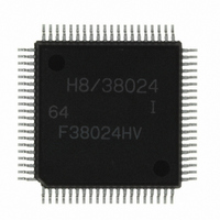
Manufacturer Part Number
HD64F38024DV
Description
IC H8/SLP MCU FLASH 80QFP
Manufacturer
Renesas Electronics America
Series
H8® H8/300L SLPr
Datasheets
1.US38024-BAG1.pdf
(684 pages)
2.DF36012GFYV.pdf
(1021 pages)
3.DF38102HV.pdf
(145 pages)
Specifications of HD64F38024DV
Core Processor
H8/300L
Core Size
8-Bit
Speed
10MHz
Connectivity
SCI
Peripherals
LCD, PWM, WDT
Number Of I /o
51
Program Memory Size
32KB (32K x 8)
Program Memory Type
FLASH
Ram Size
1K x 8
Voltage - Supply (vcc/vdd)
1.8 V ~ 5.5 V
Data Converters
A/D 8x10b
Oscillator Type
Internal
Operating Temperature
-40°C ~ 85°C
Package / Case
80-QFP
Lead Free Status / RoHS Status
Lead free / RoHS Compliant
Eeprom Size
-
Available stocks
Company
Part Number
Manufacturer
Quantity
Price
Company:

Part Number:
HD64F38024DV
Manufacturer:
Renesas Electronics America
Quantity:
10 000


Section 11 10-Bit PWM
11.3
11.3.1
When using the 10-bit PWM, set the registers in the following sequence.
1. Set PWM1 or PWM2 in PMR9 to 1 for the PWM channel to be used, so that pin P9
2. Set bits PWCRm1 and PWCRm0 in the PWM control register (PWCRm) to select a
3. Set the output waveform data in PWDRUm and PWDRLm. Be sure to write in the correct
Example: Settings in order to obtain a conversion period of 1,024 µs:
Rev. 8.00 Mar. 09, 2010 Page 392 of 658
REJ09B0042-0800
P9
conversion period of 4,096/φ (PWCRm1 = 1, PWCRm0 = 1), 2,048/φ (PWCRm1 = 1,
PWCRm0 = 0), 1,024/φ (PWCRm1 = 0, PWCRm0 = 1), or 512/φ (PWCRm1 = 0, PWCRm0 =
0). In the case of the H8/38124 Group, select between pulse-division PWM (PWCRm2 = 0)
and event counter PWM (PWCRm2 = 1) output. Refer to section 9.7, Asynchronous Event
Counter (AEC), for information on the event counter PWM (PWM incorporating AEC) output
format.
sequence, first PWDRLm then PWDRUm for the same channel. When data is written to
PWDRUm, the data will be latched in the PWM waveform generator, updating the PWM
waveform generation in synchronization with internal signals.
One conversion period consists of 4 pulses, as shown in figure 11.2. The total of the high-level
pulse widths during this period (T
This relation can be represented as follows.
where tφ is the PWM input clock period: 1/φ (PWCRm = H'0), 2/φ (PWCRm = H'1), 4/φ
(PWCRm = H'2), or 8/φ (PWCRm = H'3).
1
T
/PWM2 is designated as the PWM output pin, or both are designated as PWM output pins.
H
Operation
Operation
= (data value in PWDRUm and PWDRLm + 4) × t
When PWCRm1 = 0 and PWCRm0 = 0, the conversion period is 512/φ, so φ must be
0.5 MHz. In this case, tfn = 256 µs, with 1/2φ (resolution) = 1.0 µs.
When PWCRm1 = 0 and PWCRm0 = 1, the conversion period is 1,024/φ, so φ must be
1 MHz. In this case, tfn = 256 µs, with 1/φ (resolution) = 1.0 µs.
When PWCRm1 = 1 and PWCRm0 = 0, the conversion period is 2,048/φ , so φ must
be 2 MHz. In this case, tfn = 256 µs, with 2/φ (resolution) = 1.0 µs.
When PWCRm1 = 1 and PWCRm0 = 1, the conversion period is 4,096/φ, so φ must be
4 MHz. In this case, t
Accordingly, for a conversion period of 1,024 µs, the system clock frequency (φ) must
be 0.5 MHz, 1 MHz, 2 MHz, or 4 MHz.
fn
= 256 µs, with 4/φ (resolution) = 1.0 µs
H
) corresponds to the data in PWDRUm and PWDRLm.
φ
/2
0
/PWM1 or
Related parts for HD64F38024DV
Image
Part Number
Description
Manufacturer
Datasheet
Request
R


Part Number:
Description:
KIT STARTER FOR M16C/29
Manufacturer:
Renesas Electronics America
Datasheet:

Part Number:
Description:
KIT STARTER FOR R8C/2D
Manufacturer:
Renesas Electronics America
Datasheet:

Part Number:
Description:
R0K33062P STARTER KIT
Manufacturer:
Renesas Electronics America
Datasheet:

Part Number:
Description:
KIT STARTER FOR R8C/23 E8A
Manufacturer:
Renesas Electronics America
Datasheet:

Part Number:
Description:
KIT STARTER FOR R8C/25
Manufacturer:
Renesas Electronics America
Datasheet:

Part Number:
Description:
KIT STARTER H8S2456 SHARPE DSPLY
Manufacturer:
Renesas Electronics America
Datasheet:

Part Number:
Description:
KIT STARTER FOR R8C38C
Manufacturer:
Renesas Electronics America
Datasheet:

Part Number:
Description:
KIT STARTER FOR R8C35C
Manufacturer:
Renesas Electronics America
Datasheet:

Part Number:
Description:
KIT STARTER FOR R8CL3AC+LCD APPS
Manufacturer:
Renesas Electronics America
Datasheet:
Part Number:
Description:
KIT STARTER FOR RX610
Manufacturer:
Renesas Electronics America
Datasheet:

Part Number:
Description:
KIT STARTER FOR R32C/118
Manufacturer:
Renesas Electronics America
Datasheet:

Part Number:
Description:
KIT DEV RSK-R8C/26-29
Manufacturer:
Renesas Electronics America
Datasheet:

Part Number:
Description:
KIT STARTER FOR SH7124
Manufacturer:
Renesas Electronics America
Datasheet:

Part Number:
Description:
KIT STARTER FOR H8SX/1622
Manufacturer:
Renesas Electronics America
Datasheet: