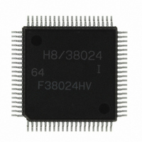
HD64F38024DV Renesas Electronics America, HD64F38024DV Datasheet - Page 93

HD64F38024DV
Manufacturer Part Number
HD64F38024DV
Description
IC H8/SLP MCU FLASH 80QFP
Manufacturer
Renesas Electronics America
Series
H8® H8/300L SLPr
Datasheets
1.US38024-BAG1.pdf
(684 pages)
2.DF36012GFYV.pdf
(1021 pages)
3.DF38102HV.pdf
(145 pages)
Specifications of HD64F38024DV
Core Processor
H8/300L
Core Size
8-Bit
Speed
10MHz
Connectivity
SCI
Peripherals
LCD, PWM, WDT
Number Of I /o
51
Program Memory Size
32KB (32K x 8)
Program Memory Type
FLASH
Ram Size
1K x 8
Voltage - Supply (vcc/vdd)
1.8 V ~ 5.5 V
Data Converters
A/D 8x10b
Oscillator Type
Internal
Operating Temperature
-40°C ~ 85°C
Package / Case
80-QFP
Lead Free Status / RoHS Status
Lead free / RoHS Compliant
Eeprom Size
-
Available stocks
Company
Part Number
Manufacturer
Quantity
Price
Company:
Part Number:
HD64F38024DV
Manufacturer:
Renesas Electronics America
Quantity:
10 000
- Current page: 93 of 684
- Download datasheet (5Mb)
2. Bit manipulation in a register containing a write-only bit
Example 3: BCLR instruction executed designating port 3 control register PCR3
As in the examples above, P3
high-level signal at P3
signals. In this example, the BCLR instruction is used to change pin P3
assumed that a high-level signal will be input to this input pin.
[A: Prior to executing BCLR]
Input/output Input
Pin state
PCR3
PDR3
[B: BCLR instruction executed]
[C: After executing BCLR]
Input/output Output
Pin state
PCR3
PDR3
[D: Explanation of how BCLR operates]
When the BCLR instruction is executed, first the CPU reads PCR3. Since PCR3 is a write-only
register, the CPU reads a value of H'FF, even though the PCR3 value is actually H'3F.
Next, the CPU clears bit 0 in the read data to 0, changing the data to H'FE. Finally, this value
(H'FE) is written to PCR3 and BCLR instruction execution ends.
As a result of this operation, bit 0 in PCR3 becomes 0, making P3
and 6 in PCR3 change to 1, so that P3
BCLR
#0
P3
Low level High level Low level Low level Low level Low level Low level Low level
0
1
P3
Low level High level Low level Low level Low level Low level Low level High level
1
1
7
7
,
@PCR3
6
. The remaining pins, P3
P3
Input
0
0
P3
Output
1
0
6
6
7
and P3
P3
Output
P3
Output
1
1
0
0
The BCLR instruction is executed designating PCR3.
5
5
6
7
are input pins, with a low-level signal input at P3
and P3
P3
Output
1
0
P3
Output
1
0
6
change from input pins to output pins.
5
4
4
to P3
0
, are output pins that output low-level
P3
Output
1
0
P3
Output
1
0
Rev. 8.00 Mar. 09, 2010 Page 71 of 658
3
3
0
an input port. However, bits 7
P3
Output
1
0
P3
Output
1
0
2
2
0
to an input port. It is
P3
Output
1
0
P3
Output
1
0
REJ09B0042-0800
1
1
Section 2 CPU
7
P3
Output
1
0
P3
Input
0
0
and a
0
0
Related parts for HD64F38024DV
Image
Part Number
Description
Manufacturer
Datasheet
Request
R

Part Number:
Description:
KIT STARTER FOR M16C/29
Manufacturer:
Renesas Electronics America
Datasheet:

Part Number:
Description:
KIT STARTER FOR R8C/2D
Manufacturer:
Renesas Electronics America
Datasheet:

Part Number:
Description:
R0K33062P STARTER KIT
Manufacturer:
Renesas Electronics America
Datasheet:

Part Number:
Description:
KIT STARTER FOR R8C/23 E8A
Manufacturer:
Renesas Electronics America
Datasheet:

Part Number:
Description:
KIT STARTER FOR R8C/25
Manufacturer:
Renesas Electronics America
Datasheet:

Part Number:
Description:
KIT STARTER H8S2456 SHARPE DSPLY
Manufacturer:
Renesas Electronics America
Datasheet:

Part Number:
Description:
KIT STARTER FOR R8C38C
Manufacturer:
Renesas Electronics America
Datasheet:

Part Number:
Description:
KIT STARTER FOR R8C35C
Manufacturer:
Renesas Electronics America
Datasheet:

Part Number:
Description:
KIT STARTER FOR R8CL3AC+LCD APPS
Manufacturer:
Renesas Electronics America
Datasheet:

Part Number:
Description:
KIT STARTER FOR RX610
Manufacturer:
Renesas Electronics America
Datasheet:

Part Number:
Description:
KIT STARTER FOR R32C/118
Manufacturer:
Renesas Electronics America
Datasheet:

Part Number:
Description:
KIT DEV RSK-R8C/26-29
Manufacturer:
Renesas Electronics America
Datasheet:

Part Number:
Description:
KIT STARTER FOR SH7124
Manufacturer:
Renesas Electronics America
Datasheet:

Part Number:
Description:
KIT STARTER FOR H8SX/1622
Manufacturer:
Renesas Electronics America
Datasheet:


