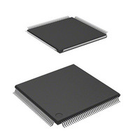
DF2166VT33WV Renesas Electronics America, DF2166VT33WV Datasheet - Page 219

DF2166VT33WV
Manufacturer Part Number
DF2166VT33WV
Description
MCU 16BIT FLASH 3V 512K 144-TQFP
Manufacturer
Renesas Electronics America
Series
H8® H8S/2100r
Datasheet
1.HS2168EPI61H-U.pdf
(876 pages)
Specifications of DF2166VT33WV
Core Processor
H8S/2000
Core Size
16-Bit
Speed
33MHz
Connectivity
I²C, IrDA, LPC, SCI, SmartCard
Peripherals
POR, PWM, WDT
Number Of I /o
106
Program Memory Size
512KB (512K x 8)
Program Memory Type
FLASH
Ram Size
40K x 8
Voltage - Supply (vcc/vdd)
3 V ~ 3.6 V
Data Converters
A/D 8x10b; D/A 2x8b
Oscillator Type
External
Operating Temperature
-20°C ~ 75°C
Package / Case
144-TQFP, 144-VQFP
Lead Free Status / RoHS Status
Lead free / RoHS Compliant
Eeprom Size
-
Available stocks
Company
Part Number
Manufacturer
Quantity
Price
Company:
Part Number:
DF2166VT33WV
Manufacturer:
Renesas Electronics America
Quantity:
135
Company:
Part Number:
DF2166VT33WV
Manufacturer:
Renesas Electronics America
Quantity:
10 000
- Current page: 219 of 876
- Download datasheet (5Mb)
Table 8.1 is a summary of the port functions. The pins of each port also function as input/output
pins of peripheral modules and interrupt input pins. Each input/output port includes a data
direction register (DDR) that controls input/output and a data register (DR) that stores output data.
DDR and DR are not provided for an input-only port.
Ports 1 to 3, 6, A, and D0 to D5 have built-in input pull-up MOSs. For port A and D0 to D5, the
on/off status of the input pull-up MOS is controlled by DDR and ODR. Ports 1 to 3 and 6 have an
input pull-up MOS control register (PCR), in addition to DDR and DR, to control the on/off status
of the input pull-up MOSs.
Ports 1 to 6, and 8 to F can drive a single TTL load and 30 pF capacitive load. All the I/O ports
can drive a Darlington transistor in output mode. Ports 8, C0 to C5 and D6 to D7 are NMOS push-
pull output.
Table 8.1
Port
Port 1
Port 2
Description
General I/O port also
functioning as PWM
output, address
output, and
address/data
multiplex input/output
General I/O port also
functioning as PWM
output, address
output, and
address/data
multiplex input/output
Port Functions
Extended Mode
(EXPE = 1)
P17/A7/AD7
P16/A6/AD6
P15/A5/AD5
P14/A4/AD4
P13/A3/AD3
P12/A2/AD2
P11/A1/AD1
P10/A0/AD0
P27/A15/AD15
P26/A14/AD14
P25/A13/AD13
P24/A12/AD12
P23/A11/AD11
P22/A10/AD10
P21/A9/AD9
P20/A8/AD8
Section 8 I/O Ports
Single-Chip Mode
(EXPE = 0)
P17/PW7
P16/PW6
P15/PW5
P14/PW4
P13/PW3
P12/PW2
P11/PW1
P10/PW0
P27/PW15
P26/PW14
P25/PW13
P24/PW12
P23/PW11
P22/PW10
P21/PW9
P20/PW8
Rev. 3.00, 03/04, page 177 of 830
I/O Status
Built-in input
pull-up MOSs
LED drive
capability
(sink current 5
mA)
Built-in input
pull-up MOSs
LED drive
capability
(sink current 5
mA)
Related parts for DF2166VT33WV
Image
Part Number
Description
Manufacturer
Datasheet
Request
R

Part Number:
Description:
KIT STARTER FOR M16C/29
Manufacturer:
Renesas Electronics America
Datasheet:

Part Number:
Description:
KIT STARTER FOR R8C/2D
Manufacturer:
Renesas Electronics America
Datasheet:

Part Number:
Description:
R0K33062P STARTER KIT
Manufacturer:
Renesas Electronics America
Datasheet:

Part Number:
Description:
KIT STARTER FOR R8C/23 E8A
Manufacturer:
Renesas Electronics America
Datasheet:

Part Number:
Description:
KIT STARTER FOR R8C/25
Manufacturer:
Renesas Electronics America
Datasheet:

Part Number:
Description:
KIT STARTER H8S2456 SHARPE DSPLY
Manufacturer:
Renesas Electronics America
Datasheet:

Part Number:
Description:
KIT STARTER FOR R8C38C
Manufacturer:
Renesas Electronics America
Datasheet:

Part Number:
Description:
KIT STARTER FOR R8C35C
Manufacturer:
Renesas Electronics America
Datasheet:

Part Number:
Description:
KIT STARTER FOR R8CL3AC+LCD APPS
Manufacturer:
Renesas Electronics America
Datasheet:

Part Number:
Description:
KIT STARTER FOR RX610
Manufacturer:
Renesas Electronics America
Datasheet:

Part Number:
Description:
KIT STARTER FOR R32C/118
Manufacturer:
Renesas Electronics America
Datasheet:

Part Number:
Description:
KIT DEV RSK-R8C/26-29
Manufacturer:
Renesas Electronics America
Datasheet:

Part Number:
Description:
KIT STARTER FOR SH7124
Manufacturer:
Renesas Electronics America
Datasheet:

Part Number:
Description:
KIT STARTER FOR H8SX/1622
Manufacturer:
Renesas Electronics America
Datasheet:

Part Number:
Description:
KIT DEV FOR SH7203
Manufacturer:
Renesas Electronics America
Datasheet:


