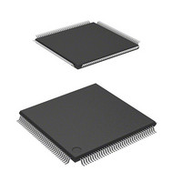
DF2166VT33WV Renesas Electronics America, DF2166VT33WV Datasheet - Page 646

DF2166VT33WV
Manufacturer Part Number
DF2166VT33WV
Description
MCU 16BIT FLASH 3V 512K 144-TQFP
Manufacturer
Renesas Electronics America
Series
H8® H8S/2100r
Datasheet
1.HS2168EPI61H-U.pdf
(876 pages)
Specifications of DF2166VT33WV
Core Processor
H8S/2000
Core Size
16-Bit
Speed
33MHz
Connectivity
I²C, IrDA, LPC, SCI, SmartCard
Peripherals
POR, PWM, WDT
Number Of I /o
106
Program Memory Size
512KB (512K x 8)
Program Memory Type
FLASH
Ram Size
40K x 8
Voltage - Supply (vcc/vdd)
3 V ~ 3.6 V
Data Converters
A/D 8x10b; D/A 2x8b
Oscillator Type
External
Operating Temperature
-20°C ~ 75°C
Package / Case
144-TQFP, 144-VQFP
Lead Free Status / RoHS Status
Lead free / RoHS Compliant
Eeprom Size
-
Available stocks
Company
Part Number
Manufacturer
Quantity
Price
Company:
Part Number:
DF2166VT33WV
Manufacturer:
Renesas Electronics America
Quantity:
135
Company:
Part Number:
DF2166VT33WV
Manufacturer:
Renesas Electronics America
Quantity:
10 000
- Current page: 646 of 876
- Download datasheet (5Mb)
18.5
The A/D converter generates an A/D conversion end interrupt (ADI) at the end of A/D conversion.
Setting the ADIE bit to 1 enables ADI interrupt requests while the ADF bit in ADCSR is set to 1
after A/D conversion ends.
The ADI interrupt can be used as a DTC activation interrupt source.
Table 18.4 A/D Converter Interrupt Source
18.6
This LSI’s A/D conversion accuracy definitions are given below.
• Resolution
•
•
•
•
•
Rev. 3.00, 03/04, page 604 of 830
Name
ADI
The number of A/D converter digital output codes
The deviation inherent in the A/D converter, given by 1/2 LSB (see figure 18.4).
The deviation of the analog input voltage value from the ideal A/D conversion characteristic
when the digital output changes from the minimum voltage value B'00 0000 0000 (H'000) to
B'00 0000 0001 (H'001) (see figure 18.5).
The deviation of the analog input voltage value from the ideal A/D conversion characteristic
when the digital output changes from B'11 1111 1110 (H'3FE) to B'11 1111 1111 (H'3FF) (see
figure 18.5).
The error with respect to the ideal A/D conversion characteristics between the zero voltage and
the full-scale voltage. Does not include the offset error, full-scale error, or quantization error
(see figure 18.5).
The deviation between the digital value and the analog input value. Includes the offset error,
full-scale error, quantization error, and nonlinearity error.
Quantization error
Offset error
Full-scale error
Nonlinearity error
Absolute accuracy
Interrupt Source
A/D Conversion Accuracy Definitions
Interrupt Source
A/D conversion end
Interrupt Flag
ADF
DTC Activation
Possible
Related parts for DF2166VT33WV
Image
Part Number
Description
Manufacturer
Datasheet
Request
R

Part Number:
Description:
KIT STARTER FOR M16C/29
Manufacturer:
Renesas Electronics America
Datasheet:

Part Number:
Description:
KIT STARTER FOR R8C/2D
Manufacturer:
Renesas Electronics America
Datasheet:

Part Number:
Description:
R0K33062P STARTER KIT
Manufacturer:
Renesas Electronics America
Datasheet:

Part Number:
Description:
KIT STARTER FOR R8C/23 E8A
Manufacturer:
Renesas Electronics America
Datasheet:

Part Number:
Description:
KIT STARTER FOR R8C/25
Manufacturer:
Renesas Electronics America
Datasheet:

Part Number:
Description:
KIT STARTER H8S2456 SHARPE DSPLY
Manufacturer:
Renesas Electronics America
Datasheet:

Part Number:
Description:
KIT STARTER FOR R8C38C
Manufacturer:
Renesas Electronics America
Datasheet:

Part Number:
Description:
KIT STARTER FOR R8C35C
Manufacturer:
Renesas Electronics America
Datasheet:

Part Number:
Description:
KIT STARTER FOR R8CL3AC+LCD APPS
Manufacturer:
Renesas Electronics America
Datasheet:

Part Number:
Description:
KIT STARTER FOR RX610
Manufacturer:
Renesas Electronics America
Datasheet:

Part Number:
Description:
KIT STARTER FOR R32C/118
Manufacturer:
Renesas Electronics America
Datasheet:

Part Number:
Description:
KIT DEV RSK-R8C/26-29
Manufacturer:
Renesas Electronics America
Datasheet:

Part Number:
Description:
KIT STARTER FOR SH7124
Manufacturer:
Renesas Electronics America
Datasheet:

Part Number:
Description:
KIT STARTER FOR H8SX/1622
Manufacturer:
Renesas Electronics America
Datasheet:

Part Number:
Description:
KIT DEV FOR SH7203
Manufacturer:
Renesas Electronics America
Datasheet:


