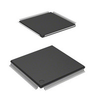
DF2166VT33WV Renesas Electronics America, DF2166VT33WV Datasheet - Page 464

DF2166VT33WV
Manufacturer Part Number
DF2166VT33WV
Description
MCU 16BIT FLASH 3V 512K 144-TQFP
Manufacturer
Renesas Electronics America
Series
H8® H8S/2100r
Datasheet
1.HS2168EPI61H-U.pdf
(876 pages)
Specifications of DF2166VT33WV
Core Processor
H8S/2000
Core Size
16-Bit
Speed
33MHz
Connectivity
I²C, IrDA, LPC, SCI, SmartCard
Peripherals
POR, PWM, WDT
Number Of I /o
106
Program Memory Size
512KB (512K x 8)
Program Memory Type
FLASH
Ram Size
40K x 8
Voltage - Supply (vcc/vdd)
3 V ~ 3.6 V
Data Converters
A/D 8x10b; D/A 2x8b
Oscillator Type
External
Operating Temperature
-20°C ~ 75°C
Package / Case
144-TQFP, 144-VQFP
Lead Free Status / RoHS Status
Lead free / RoHS Compliant
Eeprom Size
-
Available stocks
Company
Part Number
Manufacturer
Quantity
Price
Company:
Part Number:
DF2166VT33WV
Manufacturer:
Renesas Electronics America
Quantity:
135
Company:
Part Number:
DF2166VT33WV
Manufacturer:
Renesas Electronics America
Quantity:
10 000
- Current page: 464 of 876
- Download datasheet (5Mb)
14.10
Usage Notes
14.10.1 Module Stop Mode Setting
SCI operation can be disabled or enabled using the module stop control register. The initial setting
is for SCI operation to be halted. Register access is enabled by clearing module stop mode. For
details, see section 23, Power-Down Modes.
14.10.2 Break Detection and Processing
When framing error detection is performed, a break can be detected by reading the RxD pin value
directly. In a break, the input from the RxD pin becomes all 0s, and so the FER flag in SSR is set,
and the PER flag may also be set. Note that, since the SCI continues the receive operation even
after receiving a break, even if the FER flag is cleared to 0, it will be set to 1 again.
14.10.3 Mark State and Break Sending
When the TE bit in SCR is 0, the TxD pin is used as an I/O port whose direction (input or output)
and level are determined by DR and DDR of the port. This can be used to set the TxD pin to mark
state (high level) or send a break during serial data transmission. To maintain the communication
line at mark state until TE is set to 1, set both DDR and DR to 1. Since the TE bit is cleared to 0 at
this point, the TxD pin becomes an I/O port, and 1 is output from the TxD pin. To send a break
during serial transmission, first set DDR to 1 and DR to 0, and then clear the TE bit to 0. When the
TE bit is cleared to 0, the transmitter is initialized regardless of the current transmission state, the
TxD pin becomes an I/O port, and 0 is output from the TxD pin.
14.10.4 Receive Error Flags and Transmit Operations (Clock Synchronous Mode Only)
Transmission cannot be started when a receive error flag (ORER, FER, or RER) in SSR is set to 1,
even if the TDRE flag in SSR is cleared to 0. Be sure to clear the receive error flags to 0 before
starting transmission. Note also that the receive error flags cannot be cleared to 0 even if the RE
bit in SCR is cleared to 0.
14.10.5 Relation between Writing to TDR and TDRE Flag
Data can be written to TDR irrespective of the TDRE flag status in SSR. However, if the new data
is written to TDR when the TDRE flag is 0, that is, when the previous data has not been
transferred to TSR yet, the previous data in TDR is lost. Be sure to write transmit data to TDR
after verifying that the TDRE flag is set to 1.
Rev. 3.00, 03/04, page 422 of 830
Related parts for DF2166VT33WV
Image
Part Number
Description
Manufacturer
Datasheet
Request
R

Part Number:
Description:
KIT STARTER FOR M16C/29
Manufacturer:
Renesas Electronics America
Datasheet:

Part Number:
Description:
KIT STARTER FOR R8C/2D
Manufacturer:
Renesas Electronics America
Datasheet:

Part Number:
Description:
R0K33062P STARTER KIT
Manufacturer:
Renesas Electronics America
Datasheet:

Part Number:
Description:
KIT STARTER FOR R8C/23 E8A
Manufacturer:
Renesas Electronics America
Datasheet:

Part Number:
Description:
KIT STARTER FOR R8C/25
Manufacturer:
Renesas Electronics America
Datasheet:

Part Number:
Description:
KIT STARTER H8S2456 SHARPE DSPLY
Manufacturer:
Renesas Electronics America
Datasheet:

Part Number:
Description:
KIT STARTER FOR R8C38C
Manufacturer:
Renesas Electronics America
Datasheet:

Part Number:
Description:
KIT STARTER FOR R8C35C
Manufacturer:
Renesas Electronics America
Datasheet:

Part Number:
Description:
KIT STARTER FOR R8CL3AC+LCD APPS
Manufacturer:
Renesas Electronics America
Datasheet:

Part Number:
Description:
KIT STARTER FOR RX610
Manufacturer:
Renesas Electronics America
Datasheet:

Part Number:
Description:
KIT STARTER FOR R32C/118
Manufacturer:
Renesas Electronics America
Datasheet:

Part Number:
Description:
KIT DEV RSK-R8C/26-29
Manufacturer:
Renesas Electronics America
Datasheet:

Part Number:
Description:
KIT STARTER FOR SH7124
Manufacturer:
Renesas Electronics America
Datasheet:

Part Number:
Description:
KIT STARTER FOR H8SX/1622
Manufacturer:
Renesas Electronics America
Datasheet:

Part Number:
Description:
KIT DEV FOR SH7203
Manufacturer:
Renesas Electronics America
Datasheet:


