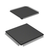
DF2166VT33WV Renesas Electronics America, DF2166VT33WV Datasheet - Page 545

DF2166VT33WV
Manufacturer Part Number
DF2166VT33WV
Description
MCU 16BIT FLASH 3V 512K 144-TQFP
Manufacturer
Renesas Electronics America
Series
H8® H8S/2100r
Datasheet
1.HS2168EPI61H-U.pdf
(876 pages)
Specifications of DF2166VT33WV
Core Processor
H8S/2000
Core Size
16-Bit
Speed
33MHz
Connectivity
I²C, IrDA, LPC, SCI, SmartCard
Peripherals
POR, PWM, WDT
Number Of I /o
106
Program Memory Size
512KB (512K x 8)
Program Memory Type
FLASH
Ram Size
40K x 8
Voltage - Supply (vcc/vdd)
3 V ~ 3.6 V
Data Converters
A/D 8x10b; D/A 2x8b
Oscillator Type
External
Operating Temperature
-20°C ~ 75°C
Package / Case
144-TQFP, 144-VQFP
Lead Free Status / RoHS Status
Lead free / RoHS Compliant
Eeprom Size
-
Available stocks
Company
Part Number
Manufacturer
Quantity
Price
Company:
Part Number:
DF2166VT33WV
Manufacturer:
Renesas Electronics America
Quantity:
135
Company:
Part Number:
DF2166VT33WV
Manufacturer:
Renesas Electronics America
Quantity:
10 000
- Current page: 545 of 876
- Download datasheet (5Mb)
Note: This restriction on usage can be canceled by setting the FNC1 and FNC0 bits to B'11 in
11. Note on ICDR register read and ICCR register access in slave transmit mode
Note: This restriction on usage can be canceled by setting the FNC1 and FNC0 bits to B'11 in
Figure 15.33 ICDR Register Read and ICCR Register Access Timing in Slave Transmit
In I
during the time shaded in figure 15.33. However, such read and write operations source no
problem in interrupt handling processing that is generated in synchronization with the rising
edge of the 9th clock pulse because the shaded time has passed before making the transition to
interrupt handling.
To handle interrupts securely, be sure to keep either of the following conditions.
Read ICDR data that has been received so far or read/write from/to ICCR before starting
Monitor the BC2 to BC0 counter in ICMR; when the count is B'000 (8th or 9th clock
2
the receive operation of the next slave address.
pulse), wait for at least two transfer clock times in order to read ICDR or read/write from/to
ICCR during the time other than the shaded time.
C bus interface slave transmit mode, do not read ICDR or do not read/write from/to ICCR
ICXR.
ICXR.
TRS bit
SDA
SCL
Address reception
R/W
8
The rise of the 9th clock is detected
Waveform at problem occurrence
A
9
ICDR read and ICCR read/write are disabled
Mode
(6 system clock period)
Rev. 3.00, 03/04, page 503 of 830
Data transmission
ICDR write
Bit 7
Related parts for DF2166VT33WV
Image
Part Number
Description
Manufacturer
Datasheet
Request
R

Part Number:
Description:
KIT STARTER FOR M16C/29
Manufacturer:
Renesas Electronics America
Datasheet:

Part Number:
Description:
KIT STARTER FOR R8C/2D
Manufacturer:
Renesas Electronics America
Datasheet:

Part Number:
Description:
R0K33062P STARTER KIT
Manufacturer:
Renesas Electronics America
Datasheet:

Part Number:
Description:
KIT STARTER FOR R8C/23 E8A
Manufacturer:
Renesas Electronics America
Datasheet:

Part Number:
Description:
KIT STARTER FOR R8C/25
Manufacturer:
Renesas Electronics America
Datasheet:

Part Number:
Description:
KIT STARTER H8S2456 SHARPE DSPLY
Manufacturer:
Renesas Electronics America
Datasheet:

Part Number:
Description:
KIT STARTER FOR R8C38C
Manufacturer:
Renesas Electronics America
Datasheet:

Part Number:
Description:
KIT STARTER FOR R8C35C
Manufacturer:
Renesas Electronics America
Datasheet:

Part Number:
Description:
KIT STARTER FOR R8CL3AC+LCD APPS
Manufacturer:
Renesas Electronics America
Datasheet:

Part Number:
Description:
KIT STARTER FOR RX610
Manufacturer:
Renesas Electronics America
Datasheet:

Part Number:
Description:
KIT STARTER FOR R32C/118
Manufacturer:
Renesas Electronics America
Datasheet:

Part Number:
Description:
KIT DEV RSK-R8C/26-29
Manufacturer:
Renesas Electronics America
Datasheet:

Part Number:
Description:
KIT STARTER FOR SH7124
Manufacturer:
Renesas Electronics America
Datasheet:

Part Number:
Description:
KIT STARTER FOR H8SX/1622
Manufacturer:
Renesas Electronics America
Datasheet:

Part Number:
Description:
KIT DEV FOR SH7203
Manufacturer:
Renesas Electronics America
Datasheet:


