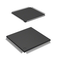
DF2166VT33WV Renesas Electronics America, DF2166VT33WV Datasheet - Page 303

DF2166VT33WV
Manufacturer Part Number
DF2166VT33WV
Description
MCU 16BIT FLASH 3V 512K 144-TQFP
Manufacturer
Renesas Electronics America
Series
H8® H8S/2100r
Datasheet
1.HS2168EPI61H-U.pdf
(876 pages)
Specifications of DF2166VT33WV
Core Processor
H8S/2000
Core Size
16-Bit
Speed
33MHz
Connectivity
I²C, IrDA, LPC, SCI, SmartCard
Peripherals
POR, PWM, WDT
Number Of I /o
106
Program Memory Size
512KB (512K x 8)
Program Memory Type
FLASH
Ram Size
40K x 8
Voltage - Supply (vcc/vdd)
3 V ~ 3.6 V
Data Converters
A/D 8x10b; D/A 2x8b
Oscillator Type
External
Operating Temperature
-20°C ~ 75°C
Package / Case
144-TQFP, 144-VQFP
Lead Free Status / RoHS Status
Lead free / RoHS Compliant
Eeprom Size
-
Available stocks
Company
Part Number
Manufacturer
Quantity
Price
Company:
Part Number:
DF2166VT33WV
Manufacturer:
Renesas Electronics America
Quantity:
135
Company:
Part Number:
DF2166VT33WV
Manufacturer:
Renesas Electronics America
Quantity:
10 000
- Current page: 303 of 876
- Download datasheet (5Mb)
This LSI has an on-chip 14-bit pulse-width modulator (PWM) timer with four output channels. It
can be connected to an external low-pass filter to operate as a 14-bit D/A converter.
10.1
• Division of pulse into multiple base cycles to reduce ripple
• Eight resolution settings
• Two base cycle settings
• Sixteen operation clocks (by combination of eight resolution settings and two base cycle
Figure 10.1 shows a block diagram of the PWM (D/A) module.
PWM1420A_010020021100
The resolution can be set to 1, 2, 64, 128, 256, 1024, 4096, or 16384 system clock cycles.
The base cycle can be set equal to T × 64 or T × 256, where T is the resolution.
settings)
PWX0
PWX1
Features
[Legend]
DACR:
DADRA:
DADRB:
DACNT:
Section 10 14-Bit PWM Timer (PWMX)
Select clock
Control
logic
PWMX D/A control register (6 bits)
PWMX D/A data register A (15 bits)
PWMX D/A data register B (15 bits)
PWMX D/A counter (14 bits)
Figure 10.1 PWMX (D/A) Block Diagram
Internal clock
Base cycle compare match A
Fine–adjustment pulse addition A
Base cycle compare match B
Fine–adjustment pulse addition B
φ
φ/2, φ/64, φ/128, φ/256,
φ/1024, φ/4096, φ/16384
Base cycle overflow
Clock
Comparator A
Comparator B
DACNT
DACR
Rev. 3.00, 03/04, page 261 of 830
DADRA
DADRB
Internal data bus
Module data bus
Bus interface
Related parts for DF2166VT33WV
Image
Part Number
Description
Manufacturer
Datasheet
Request
R

Part Number:
Description:
KIT STARTER FOR M16C/29
Manufacturer:
Renesas Electronics America
Datasheet:

Part Number:
Description:
KIT STARTER FOR R8C/2D
Manufacturer:
Renesas Electronics America
Datasheet:

Part Number:
Description:
R0K33062P STARTER KIT
Manufacturer:
Renesas Electronics America
Datasheet:

Part Number:
Description:
KIT STARTER FOR R8C/23 E8A
Manufacturer:
Renesas Electronics America
Datasheet:

Part Number:
Description:
KIT STARTER FOR R8C/25
Manufacturer:
Renesas Electronics America
Datasheet:

Part Number:
Description:
KIT STARTER H8S2456 SHARPE DSPLY
Manufacturer:
Renesas Electronics America
Datasheet:

Part Number:
Description:
KIT STARTER FOR R8C38C
Manufacturer:
Renesas Electronics America
Datasheet:

Part Number:
Description:
KIT STARTER FOR R8C35C
Manufacturer:
Renesas Electronics America
Datasheet:

Part Number:
Description:
KIT STARTER FOR R8CL3AC+LCD APPS
Manufacturer:
Renesas Electronics America
Datasheet:

Part Number:
Description:
KIT STARTER FOR RX610
Manufacturer:
Renesas Electronics America
Datasheet:

Part Number:
Description:
KIT STARTER FOR R32C/118
Manufacturer:
Renesas Electronics America
Datasheet:

Part Number:
Description:
KIT DEV RSK-R8C/26-29
Manufacturer:
Renesas Electronics America
Datasheet:

Part Number:
Description:
KIT STARTER FOR SH7124
Manufacturer:
Renesas Electronics America
Datasheet:

Part Number:
Description:
KIT STARTER FOR H8SX/1622
Manufacturer:
Renesas Electronics America
Datasheet:

Part Number:
Description:
KIT DEV FOR SH7203
Manufacturer:
Renesas Electronics America
Datasheet:


