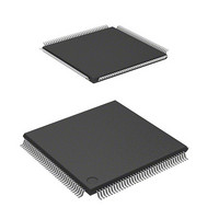
DF2166VT33WV Renesas Electronics America, DF2166VT33WV Datasheet - Page 525

DF2166VT33WV
Manufacturer Part Number
DF2166VT33WV
Description
MCU 16BIT FLASH 3V 512K 144-TQFP
Manufacturer
Renesas Electronics America
Series
H8® H8S/2100r
Datasheet
1.HS2168EPI61H-U.pdf
(876 pages)
Specifications of DF2166VT33WV
Core Processor
H8S/2000
Core Size
16-Bit
Speed
33MHz
Connectivity
I²C, IrDA, LPC, SCI, SmartCard
Peripherals
POR, PWM, WDT
Number Of I /o
106
Program Memory Size
512KB (512K x 8)
Program Memory Type
FLASH
Ram Size
40K x 8
Voltage - Supply (vcc/vdd)
3 V ~ 3.6 V
Data Converters
A/D 8x10b; D/A 2x8b
Oscillator Type
External
Operating Temperature
-20°C ~ 75°C
Package / Case
144-TQFP, 144-VQFP
Lead Free Status / RoHS Status
Lead free / RoHS Compliant
Eeprom Size
-
Available stocks
Company
Part Number
Manufacturer
Quantity
Price
Company:
Part Number:
DF2166VT33WV
Manufacturer:
Renesas Electronics America
Quantity:
135
Company:
Part Number:
DF2166VT33WV
Manufacturer:
Renesas Electronics America
Quantity:
10 000
- Current page: 525 of 876
- Download datasheet (5Mb)
The reception procedure and operations in slave receive are described below.
[1] Initialize the IIC as described in section 15.4.2, Initialization.
[2] Confirm that the ICDRF flag is 0. If the ICDRF flag is set to 1, read the ICDR and then clear
[3] When the start condition output by the master device is detected, the BBSY flag in ICCR is
[4] When the slave address matches in the first frame following the start condition, the device
[5] At the 9th clock pulse of the receive frame, the slave device returns the data in the ACKB bit
[6] At the rise of the 9th clock pulse, the IRIC flag is set to 1. If the IEIC bit has been set to 1, an
[7] At the rise of the 9th clock pulse, the receive data is transferred from ICDRS to ICDRR,
[8] Confirm that the STOP bit is cleared to 0 and clear the IRIC flag to 0.
[9] If the next read data is the third last receive frame, wait for at least one frame time to set the
[10] Confirm that the ICDRF flag is set to 1 and read ICDR. This clears the ICDRF flag to 0.
[11] At the rise of the 9th clock pulse or when the receive data is transferred from IRDRS to
[12] When the stop condition is detected (SDA is changed from low to high when SCL is high),
[13] Clear the IRIC flag to 0.
[14] Confirm that the ICDRF flag is set to 1, and read ICDR.
[15] Clear the IRIC flag.
Clear the MST and TRS bits to 0 to set slave receive mode, and set the HNDS and ACKB
bits to 0. Clear the IRIC flag in ICCR to 0 to see the end of reception.
the IRIC flag to 0.
set to 1. The master device then outputs the 7-bit slave address, and transmit/receive
direction (R/W) in synchronization with the transmit clock pulses.
operates as the slave device specified by the master device. If the 8th data bit (R/W) is 0, the
TRS bit remains cleared to 0, and slave receive operation is performed. If the 8th data bit
(R/W) is 1, the TRS bit is set to 1, and slave transmit operation is performed. When the slave
address does not match, receive operation is halted until the next start condition is detected.
as the acknowledge data.
interrupt request is sent to the CPU.
If the AASX bit has been set to 1, the IRTR flag is also set to 1.
setting the ICDRF flag to 1.
ACKB bit. Set the ACKB bit after the rise of the 9th clock pulse of the second last receive
frame.
ICDRR due to ICDR read operation, The IRIC and ICDRF flags are set to 1.
the BBSY flag is cleared to 0 and the STOP or ESTP flag is set to 1. If the STOPIM bit has
been cleared to 0, the IRIC flag is set to 1. In this case, execute step [14] to read the last
receive data.
Receive operations can be performed continuously by repeating steps [9] to [13].
Rev. 3.00, 03/04, page 483 of 830
Related parts for DF2166VT33WV
Image
Part Number
Description
Manufacturer
Datasheet
Request
R

Part Number:
Description:
KIT STARTER FOR M16C/29
Manufacturer:
Renesas Electronics America
Datasheet:

Part Number:
Description:
KIT STARTER FOR R8C/2D
Manufacturer:
Renesas Electronics America
Datasheet:

Part Number:
Description:
R0K33062P STARTER KIT
Manufacturer:
Renesas Electronics America
Datasheet:

Part Number:
Description:
KIT STARTER FOR R8C/23 E8A
Manufacturer:
Renesas Electronics America
Datasheet:

Part Number:
Description:
KIT STARTER FOR R8C/25
Manufacturer:
Renesas Electronics America
Datasheet:

Part Number:
Description:
KIT STARTER H8S2456 SHARPE DSPLY
Manufacturer:
Renesas Electronics America
Datasheet:

Part Number:
Description:
KIT STARTER FOR R8C38C
Manufacturer:
Renesas Electronics America
Datasheet:

Part Number:
Description:
KIT STARTER FOR R8C35C
Manufacturer:
Renesas Electronics America
Datasheet:

Part Number:
Description:
KIT STARTER FOR R8CL3AC+LCD APPS
Manufacturer:
Renesas Electronics America
Datasheet:

Part Number:
Description:
KIT STARTER FOR RX610
Manufacturer:
Renesas Electronics America
Datasheet:

Part Number:
Description:
KIT STARTER FOR R32C/118
Manufacturer:
Renesas Electronics America
Datasheet:

Part Number:
Description:
KIT DEV RSK-R8C/26-29
Manufacturer:
Renesas Electronics America
Datasheet:

Part Number:
Description:
KIT STARTER FOR SH7124
Manufacturer:
Renesas Electronics America
Datasheet:

Part Number:
Description:
KIT STARTER FOR H8SX/1622
Manufacturer:
Renesas Electronics America
Datasheet:

Part Number:
Description:
KIT DEV FOR SH7203
Manufacturer:
Renesas Electronics America
Datasheet:


