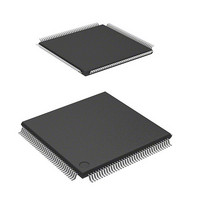
DF2166VT33WV Renesas Electronics America, DF2166VT33WV Datasheet - Page 653

DF2166VT33WV
Manufacturer Part Number
DF2166VT33WV
Description
MCU 16BIT FLASH 3V 512K 144-TQFP
Manufacturer
Renesas Electronics America
Series
H8® H8S/2100r
Datasheet
1.HS2168EPI61H-U.pdf
(876 pages)
Specifications of DF2166VT33WV
Core Processor
H8S/2000
Core Size
16-Bit
Speed
33MHz
Connectivity
I²C, IrDA, LPC, SCI, SmartCard
Peripherals
POR, PWM, WDT
Number Of I /o
106
Program Memory Size
512KB (512K x 8)
Program Memory Type
FLASH
Ram Size
40K x 8
Voltage - Supply (vcc/vdd)
3 V ~ 3.6 V
Data Converters
A/D 8x10b; D/A 2x8b
Oscillator Type
External
Operating Temperature
-20°C ~ 75°C
Package / Case
144-TQFP, 144-VQFP
Lead Free Status / RoHS Status
Lead free / RoHS Compliant
Eeprom Size
-
Available stocks
Company
Part Number
Manufacturer
Quantity
Price
Company:
Part Number:
DF2166VT33WV
Manufacturer:
Renesas Electronics America
Quantity:
135
Company:
Part Number:
DF2166VT33WV
Manufacturer:
Renesas Electronics America
Quantity:
10 000
- Current page: 653 of 876
- Download datasheet (5Mb)
The flash memory has the following features. Figure 20.1 shows a block diagram of the flash
memory.
20.1
• Size
Product Classification
H8S/2168
H8S/2167
H8S/2166
• Two flash-memory MATs according to LSI initiation mode
• Programming/erasing interface by the download of on-chip program
• Programming/erasing time
• Number of programming
• Three on-board programming modes
ROM1250A_000020030700
The on-chip flash memory has two memory spaces in the same address space (hereafter
referred to as memory MATs). The mode setting in the initiation determines which memory
MAT is initiated first. The MAT can be switched by using the bank-switching method after
initiation.
The user memory MAT is initiated at a power-on reset in user mode: 256 kbytes
The user boot memory MAT is initiated at a power-on reset in user boot mode: 8 kbytes
This LSI has a dedicated programming/erasing program. After downloading this program to
the on-chip RAM, programming/erasing can be performed by setting the argument parameter.
The flash memory programming time is 3 ms (typ) in 128-byte simultaneous programming and
approximately 25 µs per byte. The erasing time is 1000 ms (typ) per 64-kbyte block.
The number of flash memory programming can be up to 100 times at the minimum. (The value
ranged from 1 to 100 is guaranteed.)
Boot mode
User program mode
Section 20 Flash Memory (0.18-µm F-ZTAT Version)
(H8S/2168), 384 kbytes (H8S/2167), 512 kbytes (H8S/2166)
This mode is a program mode that uses an on-chip SCI interface. The user MAT and user
boot MAT can be programmed. This mode can automatically adjust the bit rate between
host and this LSI.
The user MAT can be programmed by using the optional interface.
Features
HD64F2168
HD64F2167
HD64F2166
ROM Size
256 kbytes
384 kbytes
512 kbytes
ROM Address
H'000000 to H'03FFFF
H'000000 to H'05FFFF
H'000000 to H'07FFFF
Rev. 3.00, 03/04, page 611 of 830
Related parts for DF2166VT33WV
Image
Part Number
Description
Manufacturer
Datasheet
Request
R

Part Number:
Description:
KIT STARTER FOR M16C/29
Manufacturer:
Renesas Electronics America
Datasheet:

Part Number:
Description:
KIT STARTER FOR R8C/2D
Manufacturer:
Renesas Electronics America
Datasheet:

Part Number:
Description:
R0K33062P STARTER KIT
Manufacturer:
Renesas Electronics America
Datasheet:

Part Number:
Description:
KIT STARTER FOR R8C/23 E8A
Manufacturer:
Renesas Electronics America
Datasheet:

Part Number:
Description:
KIT STARTER FOR R8C/25
Manufacturer:
Renesas Electronics America
Datasheet:

Part Number:
Description:
KIT STARTER H8S2456 SHARPE DSPLY
Manufacturer:
Renesas Electronics America
Datasheet:

Part Number:
Description:
KIT STARTER FOR R8C38C
Manufacturer:
Renesas Electronics America
Datasheet:

Part Number:
Description:
KIT STARTER FOR R8C35C
Manufacturer:
Renesas Electronics America
Datasheet:

Part Number:
Description:
KIT STARTER FOR R8CL3AC+LCD APPS
Manufacturer:
Renesas Electronics America
Datasheet:

Part Number:
Description:
KIT STARTER FOR RX610
Manufacturer:
Renesas Electronics America
Datasheet:

Part Number:
Description:
KIT STARTER FOR R32C/118
Manufacturer:
Renesas Electronics America
Datasheet:

Part Number:
Description:
KIT DEV RSK-R8C/26-29
Manufacturer:
Renesas Electronics America
Datasheet:

Part Number:
Description:
KIT STARTER FOR SH7124
Manufacturer:
Renesas Electronics America
Datasheet:

Part Number:
Description:
KIT STARTER FOR H8SX/1622
Manufacturer:
Renesas Electronics America
Datasheet:

Part Number:
Description:
KIT DEV FOR SH7203
Manufacturer:
Renesas Electronics America
Datasheet:


