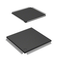
DF2166VT33WV Renesas Electronics America, DF2166VT33WV Datasheet - Page 30

DF2166VT33WV
Manufacturer Part Number
DF2166VT33WV
Description
MCU 16BIT FLASH 3V 512K 144-TQFP
Manufacturer
Renesas Electronics America
Series
H8® H8S/2100r
Datasheet
1.HS2168EPI61H-U.pdf
(876 pages)
Specifications of DF2166VT33WV
Core Processor
H8S/2000
Core Size
16-Bit
Speed
33MHz
Connectivity
I²C, IrDA, LPC, SCI, SmartCard
Peripherals
POR, PWM, WDT
Number Of I /o
106
Program Memory Size
512KB (512K x 8)
Program Memory Type
FLASH
Ram Size
40K x 8
Voltage - Supply (vcc/vdd)
3 V ~ 3.6 V
Data Converters
A/D 8x10b; D/A 2x8b
Oscillator Type
External
Operating Temperature
-20°C ~ 75°C
Package / Case
144-TQFP, 144-VQFP
Lead Free Status / RoHS Status
Lead free / RoHS Compliant
Eeprom Size
-
Available stocks
Company
Part Number
Manufacturer
Quantity
Price
Company:
Part Number:
DF2166VT33WV
Manufacturer:
Renesas Electronics America
Quantity:
135
Company:
Part Number:
DF2166VT33WV
Manufacturer:
Renesas Electronics America
Quantity:
10 000
- Current page: 30 of 876
- Download datasheet (5Mb)
Section 12 8-Bit Timer (TMR)
Figure 12.1 Block Diagram of 8-Bit Timer (TMR_0 and TMR_1)............................................ 306
Figure 12.2 Block Diagram of 8-Bit Timer (TMR_Y and TMR_X).......................................... 307
Figure 12.3 Pulse Output Example ............................................................................................. 322
Figure 12.4 Count Timing for Internal Clock Input ................................................................... 323
Figure 12.5 Count Timing for External Clock Input .................................................................. 323
Figure 12.6 Timing of CMF Setting at Compare-Match ............................................................ 324
Figure 12.7 Timing of Toggled Timer Output by Compare-Match A Signal............................. 324
Figure 12.8 Timing of Counter Clear by Compare-Match ......................................................... 324
Figure 12.9 Timing of Counter Clear by External Reset Input................................................... 325
Figure 12.10 Timing of OVF Flag Setting ................................................................................. 325
Figure 12.11 Timing of Input Capture Operation....................................................................... 327
Figure 12.12 Timing of Input Capture Signal
Figure 12.13 Conflict between TCNT Write and Counter Clear ................................................ 330
Figure 12.14 Conflict between TCNT Write and Increment ...................................................... 331
Figure 12.15 Conflict between TCOR Write and Compare-Match ............................................ 332
Section 13 Watchdog Timer (WDT)
Figure 13.1 Block Diagram of WDT .......................................................................................... 338
Figure 13.2 Watchdog Timer Mode (RST/NMI = 1) Operation................................................. 344
Figure 13.3 Interval Timer Mode Operation............................................................................... 345
Figure 13.4 OVF Flag Set Timing .............................................................................................. 345
Figure 13.5 Output Timing of RESO signal ............................................................................... 346
Figure 13.6 Writing to TCNT and TCSR (WDT_0)................................................................... 348
Figure 13.7 Conflict between TCNT Write and Increment ........................................................ 349
Figure 13.8 Sample Circuit for Resetting the System by the RESO Signal................................ 350
Section 14 Serial Communication Interface (SCI, IrDA, and CRC)
Figure 14.1 Block Diagram of SCI_1......................................................................................... 353
Figure 14.2 Block Diagram of SCI_0 and SCI_2 ....................................................................... 354
Figure 14.3 Data Format in Asynchronous Communication
Figure 14.4 Receive Data Sampling Timing in Asynchronous Mode ........................................ 382
Figure 14.5 Relation between Output Clock and Transmit Data Phase
Figure 14.6 Basic Clock Examples When Average Transfer Rate is Selected (1) ..................... 384
Figure 14.7 Basic Clock Examples When Average Transfer Rate is Selected (2) ..................... 385
Figure 14.8 Sample SCI Initialization Flowchart ....................................................................... 386
Figure 14.9 Example of Operation in Transmission in Asynchronous Mode
Figure 14.10 Sample Serial Transmission Flowchart ................................................................. 388
Rev. 3.00, 03/04, page xxviii of xl
(Example with 8-Bit Data, Parity, Two Stop Bits)................................................... 380
(Asynchronous Mode).............................................................................................. 383
(Example with 8-Bit Data, Parity, One Stop Bit)..................................................... 387
(Input capture signal is input during TICRR and TICRF read) ............................. 328
Related parts for DF2166VT33WV
Image
Part Number
Description
Manufacturer
Datasheet
Request
R

Part Number:
Description:
KIT STARTER FOR M16C/29
Manufacturer:
Renesas Electronics America
Datasheet:

Part Number:
Description:
KIT STARTER FOR R8C/2D
Manufacturer:
Renesas Electronics America
Datasheet:

Part Number:
Description:
R0K33062P STARTER KIT
Manufacturer:
Renesas Electronics America
Datasheet:

Part Number:
Description:
KIT STARTER FOR R8C/23 E8A
Manufacturer:
Renesas Electronics America
Datasheet:

Part Number:
Description:
KIT STARTER FOR R8C/25
Manufacturer:
Renesas Electronics America
Datasheet:

Part Number:
Description:
KIT STARTER H8S2456 SHARPE DSPLY
Manufacturer:
Renesas Electronics America
Datasheet:

Part Number:
Description:
KIT STARTER FOR R8C38C
Manufacturer:
Renesas Electronics America
Datasheet:

Part Number:
Description:
KIT STARTER FOR R8C35C
Manufacturer:
Renesas Electronics America
Datasheet:

Part Number:
Description:
KIT STARTER FOR R8CL3AC+LCD APPS
Manufacturer:
Renesas Electronics America
Datasheet:

Part Number:
Description:
KIT STARTER FOR RX610
Manufacturer:
Renesas Electronics America
Datasheet:

Part Number:
Description:
KIT STARTER FOR R32C/118
Manufacturer:
Renesas Electronics America
Datasheet:

Part Number:
Description:
KIT DEV RSK-R8C/26-29
Manufacturer:
Renesas Electronics America
Datasheet:

Part Number:
Description:
KIT STARTER FOR SH7124
Manufacturer:
Renesas Electronics America
Datasheet:

Part Number:
Description:
KIT STARTER FOR H8SX/1622
Manufacturer:
Renesas Electronics America
Datasheet:

Part Number:
Description:
KIT DEV FOR SH7203
Manufacturer:
Renesas Electronics America
Datasheet:


