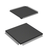
DF2166VT33WV Renesas Electronics America, DF2166VT33WV Datasheet - Page 767

DF2166VT33WV
Manufacturer Part Number
DF2166VT33WV
Description
MCU 16BIT FLASH 3V 512K 144-TQFP
Manufacturer
Renesas Electronics America
Series
H8® H8S/2100r
Datasheet
1.HS2168EPI61H-U.pdf
(876 pages)
Specifications of DF2166VT33WV
Core Processor
H8S/2000
Core Size
16-Bit
Speed
33MHz
Connectivity
I²C, IrDA, LPC, SCI, SmartCard
Peripherals
POR, PWM, WDT
Number Of I /o
106
Program Memory Size
512KB (512K x 8)
Program Memory Type
FLASH
Ram Size
40K x 8
Voltage - Supply (vcc/vdd)
3 V ~ 3.6 V
Data Converters
A/D 8x10b; D/A 2x8b
Oscillator Type
External
Operating Temperature
-20°C ~ 75°C
Package / Case
144-TQFP, 144-VQFP
Lead Free Status / RoHS Status
Lead free / RoHS Compliant
Eeprom Size
-
Available stocks
Company
Part Number
Manufacturer
Quantity
Price
Company:
Part Number:
DF2166VT33WV
Manufacturer:
Renesas Electronics America
Quantity:
135
Company:
Part Number:
DF2166VT33WV
Manufacturer:
Renesas Electronics America
Quantity:
10 000
- Current page: 767 of 876
- Download datasheet (5Mb)
22.7
The clock select circuit selects the system clock that is used in this LSI.
A clock generated by the oscillator, to which the EXTAL and XTAL pins are input, and multiplied
by the PLL circuit is selected as a system clock when returning from high-speed mode, medium-
speed mode, sleep mode, the reset state, or standby mode.
In subactive mode, subsleep mode, or watch mode, a subclock input from the EXCL pin is
selected as a system clock when the EXCLE bit in LPWRCR is 1. At this time, modules such as
the CPU, TMR_0, TMR_1, WDT_0, WDT_1, ports, and interrupt controller and their functions
operate on the φSUB. The count clock and sampling clock for each timer are divided φSUB
clocks.
22.8
22.8.1
Since all kinds of characteristics of the resonator are closely related to the board design by the
user, use the example of resonator connection in this document for only reference; be sure to use
an resonator that has been sufficiently evaluated by the user. Consult with the resonator
manufacturer about the resonator circuit ratings which vary depending on the stray capacitances of
the resonator and installation circuit. Make sure the voltage applied to the oscillation pins do not
exceed the maximum rating.
22.8.2
When using a crystal resonator, the crystal resonator and its load capacitors should be placed as
close as possible to the EXTAL and XTAL pins. Other signal lines should be routed away from
the oscillation circuit to prevent inductive interference with the correct oscillation as shown in
figure 22.5.
Clock Select Circuit
Usage Notes
Note on Resonator
Notes on Board Design
Figure 22.5 Note on Board Design of Oscillation Circuit Section
Prohibited
C
C
L2
L1
Signal A Signal B
XTAL
EXTAL
This LSI
Rev. 3.00, 03/04, page 725 of 830
Related parts for DF2166VT33WV
Image
Part Number
Description
Manufacturer
Datasheet
Request
R

Part Number:
Description:
KIT STARTER FOR M16C/29
Manufacturer:
Renesas Electronics America
Datasheet:

Part Number:
Description:
KIT STARTER FOR R8C/2D
Manufacturer:
Renesas Electronics America
Datasheet:

Part Number:
Description:
R0K33062P STARTER KIT
Manufacturer:
Renesas Electronics America
Datasheet:

Part Number:
Description:
KIT STARTER FOR R8C/23 E8A
Manufacturer:
Renesas Electronics America
Datasheet:

Part Number:
Description:
KIT STARTER FOR R8C/25
Manufacturer:
Renesas Electronics America
Datasheet:

Part Number:
Description:
KIT STARTER H8S2456 SHARPE DSPLY
Manufacturer:
Renesas Electronics America
Datasheet:

Part Number:
Description:
KIT STARTER FOR R8C38C
Manufacturer:
Renesas Electronics America
Datasheet:

Part Number:
Description:
KIT STARTER FOR R8C35C
Manufacturer:
Renesas Electronics America
Datasheet:

Part Number:
Description:
KIT STARTER FOR R8CL3AC+LCD APPS
Manufacturer:
Renesas Electronics America
Datasheet:

Part Number:
Description:
KIT STARTER FOR RX610
Manufacturer:
Renesas Electronics America
Datasheet:

Part Number:
Description:
KIT STARTER FOR R32C/118
Manufacturer:
Renesas Electronics America
Datasheet:

Part Number:
Description:
KIT DEV RSK-R8C/26-29
Manufacturer:
Renesas Electronics America
Datasheet:

Part Number:
Description:
KIT STARTER FOR SH7124
Manufacturer:
Renesas Electronics America
Datasheet:

Part Number:
Description:
KIT STARTER FOR H8SX/1622
Manufacturer:
Renesas Electronics America
Datasheet:

Part Number:
Description:
KIT DEV FOR SH7203
Manufacturer:
Renesas Electronics America
Datasheet:


