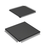
DF2166VT33WV Renesas Electronics America, DF2166VT33WV Datasheet - Page 690

DF2166VT33WV
Manufacturer Part Number
DF2166VT33WV
Description
MCU 16BIT FLASH 3V 512K 144-TQFP
Manufacturer
Renesas Electronics America
Series
H8® H8S/2100r
Datasheet
1.HS2168EPI61H-U.pdf
(876 pages)
Specifications of DF2166VT33WV
Core Processor
H8S/2000
Core Size
16-Bit
Speed
33MHz
Connectivity
I²C, IrDA, LPC, SCI, SmartCard
Peripherals
POR, PWM, WDT
Number Of I /o
106
Program Memory Size
512KB (512K x 8)
Program Memory Type
FLASH
Ram Size
40K x 8
Voltage - Supply (vcc/vdd)
3 V ~ 3.6 V
Data Converters
A/D 8x10b; D/A 2x8b
Oscillator Type
External
Operating Temperature
-20°C ~ 75°C
Package / Case
144-TQFP, 144-VQFP
Lead Free Status / RoHS Status
Lead free / RoHS Compliant
Eeprom Size
-
Available stocks
Company
Part Number
Manufacturer
Quantity
Price
Company:
Part Number:
DF2166VT33WV
Manufacturer:
Renesas Electronics America
Quantity:
135
Company:
Part Number:
DF2166VT33WV
Manufacturer:
Renesas Electronics America
Quantity:
10 000
- Current page: 690 of 876
- Download datasheet (5Mb)
12. Programming
13. The return value in the programming program, FPFR (general register R0L) is determined.
14. Determine whether programming of the necessary data has finished.
15. After programming finishes, clear FKEY and specify software protection.
Rev. 3.00, 03/04, page 648 of 830
Example of the FMPDR setting
There is an entry point of the programming program in the area from the start address specified
by FTDAR + 16 bytes of the on-chip RAM. The subroutine is called and programming is
executed by using the following steps.
MOV.L
JSR
NOP
The general registers other than R0L are held in the programming program.
R0L is a return value of the FPFR parameter.
Since the stack area is used in the programming program, a stack area of 128 bytes at the
If more than 128 bytes of data are to be programmed, specify FMPAR and FMPDR in 128-
byte units, and repeat steps 12 to 14. Increment the programming destination address by 128
bytes and update the programming data pointer correctly. If an address which has already been
programmed is written to again, not only will a programming error occur, but also flash
memory will be damaged.
If this LSI is restarted by a reset immediately after user MAT programming has finished,
secure the reset period (period of RES = 0) of 100 µs which is longer than normal.
When the storage destination of the program data is flash memory, even if the program
execution routine is executed, programming is not executed and an error is returned to the
FPFR parameter. In this case, the program data must be transferred to the on-chip RAM
and then programming must be executed.
maximum must be allocated in RAM.
#DLTOP+16,ER2
@ER2
; Set entry address to ER2
; Call programming routine
Related parts for DF2166VT33WV
Image
Part Number
Description
Manufacturer
Datasheet
Request
R

Part Number:
Description:
KIT STARTER FOR M16C/29
Manufacturer:
Renesas Electronics America
Datasheet:

Part Number:
Description:
KIT STARTER FOR R8C/2D
Manufacturer:
Renesas Electronics America
Datasheet:

Part Number:
Description:
R0K33062P STARTER KIT
Manufacturer:
Renesas Electronics America
Datasheet:

Part Number:
Description:
KIT STARTER FOR R8C/23 E8A
Manufacturer:
Renesas Electronics America
Datasheet:

Part Number:
Description:
KIT STARTER FOR R8C/25
Manufacturer:
Renesas Electronics America
Datasheet:

Part Number:
Description:
KIT STARTER H8S2456 SHARPE DSPLY
Manufacturer:
Renesas Electronics America
Datasheet:

Part Number:
Description:
KIT STARTER FOR R8C38C
Manufacturer:
Renesas Electronics America
Datasheet:

Part Number:
Description:
KIT STARTER FOR R8C35C
Manufacturer:
Renesas Electronics America
Datasheet:

Part Number:
Description:
KIT STARTER FOR R8CL3AC+LCD APPS
Manufacturer:
Renesas Electronics America
Datasheet:

Part Number:
Description:
KIT STARTER FOR RX610
Manufacturer:
Renesas Electronics America
Datasheet:

Part Number:
Description:
KIT STARTER FOR R32C/118
Manufacturer:
Renesas Electronics America
Datasheet:

Part Number:
Description:
KIT DEV RSK-R8C/26-29
Manufacturer:
Renesas Electronics America
Datasheet:

Part Number:
Description:
KIT STARTER FOR SH7124
Manufacturer:
Renesas Electronics America
Datasheet:

Part Number:
Description:
KIT STARTER FOR H8SX/1622
Manufacturer:
Renesas Electronics America
Datasheet:

Part Number:
Description:
KIT DEV FOR SH7203
Manufacturer:
Renesas Electronics America
Datasheet:


