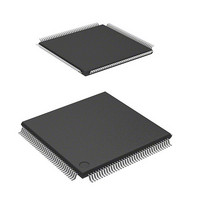
DF2166VT33WV Renesas Electronics America, DF2166VT33WV Datasheet - Page 449

DF2166VT33WV
Manufacturer Part Number
DF2166VT33WV
Description
MCU 16BIT FLASH 3V 512K 144-TQFP
Manufacturer
Renesas Electronics America
Series
H8® H8S/2100r
Datasheet
1.HS2168EPI61H-U.pdf
(876 pages)
Specifications of DF2166VT33WV
Core Processor
H8S/2000
Core Size
16-Bit
Speed
33MHz
Connectivity
I²C, IrDA, LPC, SCI, SmartCard
Peripherals
POR, PWM, WDT
Number Of I /o
106
Program Memory Size
512KB (512K x 8)
Program Memory Type
FLASH
Ram Size
40K x 8
Voltage - Supply (vcc/vdd)
3 V ~ 3.6 V
Data Converters
A/D 8x10b; D/A 2x8b
Oscillator Type
External
Operating Temperature
-20°C ~ 75°C
Package / Case
144-TQFP, 144-VQFP
Lead Free Status / RoHS Status
Lead free / RoHS Compliant
Eeprom Size
-
Available stocks
Company
Part Number
Manufacturer
Quantity
Price
Company:
Part Number:
DF2166VT33WV
Manufacturer:
Renesas Electronics America
Quantity:
135
Company:
Part Number:
DF2166VT33WV
Manufacturer:
Renesas Electronics America
Quantity:
10 000
- Current page: 449 of 876
- Download datasheet (5Mb)
14.7
The SCI supports the IC card (smart card) interface based on the ISO/IEC 7816-3 (Identification
Card) standard as an enhanced serial communication interface function. Smart card interface mode
can be selected using the appropriate register.
14.7.1
Figure 14.24 shows a sample connection between the smart card and this LSI. As in the figure,
since this LSI communicates with the IC card using a single transmission line, interconnect the
TxD and RxD pins and pull up the data transmission line to VCC using a resistor. Setting the RE
and TE bits in SCR to 1 with the IC card not connected enables closed transmission/reception
allowing self diagnosis. To supply the IC card with the clock pulses generated by the SCI, input
the SCK pin output to the CLK pin of the IC card. A reset signal can be supplied via the output
port of this LSI.
14.7.2
Figure 14.25 shows the data transfer formats in smart card interface mode.
• One frame contains 8-bit data and a parity bit in asynchronous mode.
• During transmission, at least 2 etu (elementary time unit: time required for transferring one bit)
• If a parity error is detected during reception, a low error signal is output for 1 etu after 10.5 etu
• If an error signal is sampled during transmission, the same data is automatically re-transmitted
is secured as a guard time after the end of the parity bit before the start of the next frame.
has passed from the start bit.
after two or more etu.
Smart Card Interface Description
Sample Connection
Data Format (Except in Block Transfer Mode)
Figure 14.24 Pin Connection for Smart Card Interface
Main unit of the device
to be connected
Rx (port)
This LSI
SCK
RxD
TxD
Reset line
Clock line
Data line
VCC
Rev. 3.00, 03/04, page 407 of 830
I/O
CLK
RST
IC card
Related parts for DF2166VT33WV
Image
Part Number
Description
Manufacturer
Datasheet
Request
R

Part Number:
Description:
KIT STARTER FOR M16C/29
Manufacturer:
Renesas Electronics America
Datasheet:

Part Number:
Description:
KIT STARTER FOR R8C/2D
Manufacturer:
Renesas Electronics America
Datasheet:

Part Number:
Description:
R0K33062P STARTER KIT
Manufacturer:
Renesas Electronics America
Datasheet:

Part Number:
Description:
KIT STARTER FOR R8C/23 E8A
Manufacturer:
Renesas Electronics America
Datasheet:

Part Number:
Description:
KIT STARTER FOR R8C/25
Manufacturer:
Renesas Electronics America
Datasheet:

Part Number:
Description:
KIT STARTER H8S2456 SHARPE DSPLY
Manufacturer:
Renesas Electronics America
Datasheet:

Part Number:
Description:
KIT STARTER FOR R8C38C
Manufacturer:
Renesas Electronics America
Datasheet:

Part Number:
Description:
KIT STARTER FOR R8C35C
Manufacturer:
Renesas Electronics America
Datasheet:

Part Number:
Description:
KIT STARTER FOR R8CL3AC+LCD APPS
Manufacturer:
Renesas Electronics America
Datasheet:

Part Number:
Description:
KIT STARTER FOR RX610
Manufacturer:
Renesas Electronics America
Datasheet:

Part Number:
Description:
KIT STARTER FOR R32C/118
Manufacturer:
Renesas Electronics America
Datasheet:

Part Number:
Description:
KIT DEV RSK-R8C/26-29
Manufacturer:
Renesas Electronics America
Datasheet:

Part Number:
Description:
KIT STARTER FOR SH7124
Manufacturer:
Renesas Electronics America
Datasheet:

Part Number:
Description:
KIT STARTER FOR H8SX/1622
Manufacturer:
Renesas Electronics America
Datasheet:

Part Number:
Description:
KIT DEV FOR SH7203
Manufacturer:
Renesas Electronics America
Datasheet:


