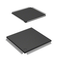
DF2166VT33WV Renesas Electronics America, DF2166VT33WV Datasheet - Page 758

DF2166VT33WV
Manufacturer Part Number
DF2166VT33WV
Description
MCU 16BIT FLASH 3V 512K 144-TQFP
Manufacturer
Renesas Electronics America
Series
H8® H8S/2100r
Datasheet
1.HS2168EPI61H-U.pdf
(876 pages)
Specifications of DF2166VT33WV
Core Processor
H8S/2000
Core Size
16-Bit
Speed
33MHz
Connectivity
I²C, IrDA, LPC, SCI, SmartCard
Peripherals
POR, PWM, WDT
Number Of I /o
106
Program Memory Size
512KB (512K x 8)
Program Memory Type
FLASH
Ram Size
40K x 8
Voltage - Supply (vcc/vdd)
3 V ~ 3.6 V
Data Converters
A/D 8x10b; D/A 2x8b
Oscillator Type
External
Operating Temperature
-20°C ~ 75°C
Package / Case
144-TQFP, 144-VQFP
Lead Free Status / RoHS Status
Lead free / RoHS Compliant
Eeprom Size
-
Available stocks
Company
Part Number
Manufacturer
Quantity
Price
Company:
Part Number:
DF2166VT33WV
Manufacturer:
Renesas Electronics America
Quantity:
135
Company:
Part Number:
DF2166VT33WV
Manufacturer:
Renesas Electronics America
Quantity:
10 000
- Current page: 758 of 876
- Download datasheet (5Mb)
EXTEST: Instruction code: B'0000
The EXTEST instruction is provided to test external circuitry when this LSI is mounted on a
printed circuit board. When this instruction is executed, output pins are used to output test data
(previously set by the SAMPLE/PRELOAD instruction) from the boundary scan register to the
printed circuit board, and input pins are used to latch test results into the boundary scan register
from the printed circuit board. If testing is carried out by using the EXTEST instruction N times,
the Nth test data is scanned in when test data (N-1) is scanned out.
Data loaded into the output pin boundary scan register in the Capture-DR state is not used for
external circuit testing (it is replaced by a shift operation).
CLAMP: Instruction code: B'0010
When the CLAMP instruction is enabled, the output pin outputs the value of the boundary scan
register that has been previously set by the SAMPLE/PRELOAD instruction. While the CLAMP
instruction is enabled, the state of the boundary scan register maintains the previous state
regardless of the state of the TAP controller.
A bypass register is connected between the ETDI and ETDO pins. The related circuit operates in
the same way when the BYPASS instruction is enabled.
HIGHZ: Instruction code: B'0011
When the HIGHZ instruction is enabled, all output pins enter a high-impedance state. While the
HIGHZ instruction is enabled, the state of the boundary scan register maintains the previous state
regardless of the state of the TAP controller.
A bypass register is connected between the ETDI and ETDO pins. The related circuit operates in
the same way when the BYPASS instruction is enabled.
IDCODE: Instruction code: B'1110
When the IDCODE instruction is enabled, the value of the ID code register is output from the
ETDO pin with LSB first when the TAP controller is in the Shift-DR state. While the IDCODE
instruction is being executed, the test circuit does not affect the system circuit.
When the TAP controller is in the Test-Logic-Reset state, the instruction register is initialized to
the IDCODE instruction.
Rev. 3.00, 03/04, page 716 of 830
Related parts for DF2166VT33WV
Image
Part Number
Description
Manufacturer
Datasheet
Request
R

Part Number:
Description:
KIT STARTER FOR M16C/29
Manufacturer:
Renesas Electronics America
Datasheet:

Part Number:
Description:
KIT STARTER FOR R8C/2D
Manufacturer:
Renesas Electronics America
Datasheet:

Part Number:
Description:
R0K33062P STARTER KIT
Manufacturer:
Renesas Electronics America
Datasheet:

Part Number:
Description:
KIT STARTER FOR R8C/23 E8A
Manufacturer:
Renesas Electronics America
Datasheet:

Part Number:
Description:
KIT STARTER FOR R8C/25
Manufacturer:
Renesas Electronics America
Datasheet:

Part Number:
Description:
KIT STARTER H8S2456 SHARPE DSPLY
Manufacturer:
Renesas Electronics America
Datasheet:

Part Number:
Description:
KIT STARTER FOR R8C38C
Manufacturer:
Renesas Electronics America
Datasheet:

Part Number:
Description:
KIT STARTER FOR R8C35C
Manufacturer:
Renesas Electronics America
Datasheet:

Part Number:
Description:
KIT STARTER FOR R8CL3AC+LCD APPS
Manufacturer:
Renesas Electronics America
Datasheet:

Part Number:
Description:
KIT STARTER FOR RX610
Manufacturer:
Renesas Electronics America
Datasheet:

Part Number:
Description:
KIT STARTER FOR R32C/118
Manufacturer:
Renesas Electronics America
Datasheet:

Part Number:
Description:
KIT DEV RSK-R8C/26-29
Manufacturer:
Renesas Electronics America
Datasheet:

Part Number:
Description:
KIT STARTER FOR SH7124
Manufacturer:
Renesas Electronics America
Datasheet:

Part Number:
Description:
KIT STARTER FOR H8SX/1622
Manufacturer:
Renesas Electronics America
Datasheet:

Part Number:
Description:
KIT DEV FOR SH7203
Manufacturer:
Renesas Electronics America
Datasheet:


