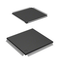
DF2166VT33WV Renesas Electronics America, DF2166VT33WV Datasheet - Page 778

DF2166VT33WV
Manufacturer Part Number
DF2166VT33WV
Description
MCU 16BIT FLASH 3V 512K 144-TQFP
Manufacturer
Renesas Electronics America
Series
H8® H8S/2100r
Datasheet
1.HS2168EPI61H-U.pdf
(876 pages)
Specifications of DF2166VT33WV
Core Processor
H8S/2000
Core Size
16-Bit
Speed
33MHz
Connectivity
I²C, IrDA, LPC, SCI, SmartCard
Peripherals
POR, PWM, WDT
Number Of I /o
106
Program Memory Size
512KB (512K x 8)
Program Memory Type
FLASH
Ram Size
40K x 8
Voltage - Supply (vcc/vdd)
3 V ~ 3.6 V
Data Converters
A/D 8x10b; D/A 2x8b
Oscillator Type
External
Operating Temperature
-20°C ~ 75°C
Package / Case
144-TQFP, 144-VQFP
Lead Free Status / RoHS Status
Lead free / RoHS Compliant
Eeprom Size
-
Available stocks
Company
Part Number
Manufacturer
Quantity
Price
Company:
Part Number:
DF2166VT33WV
Manufacturer:
Renesas Electronics America
Quantity:
135
Company:
Part Number:
DF2166VT33WV
Manufacturer:
Renesas Electronics America
Quantity:
10 000
- Current page: 778 of 876
- Download datasheet (5Mb)
Rev. 3.00, 03/04, page 736 of 830
Notes:
Program execution state
SLEEP instruction
SSBY = 1, PSS = 1,
DTON = 1, LSON = 0
After the oscillation
stabilization time
(STS2 to STS0), clock
switching exception
processing
• When a transition is made between modes by means of an interrupt, the transition cannot be made
• Always select high-speed mode before making a transition to watch mode or sub-active mode.
1.
2.
3.
on interrupt source generation alone. Ensure that interrupt handling is performed after accepting the
interrupt request.
NMI, IRQ0 to IRQ15, KIN0 to KIN15, WUE8 to WUE15, and WDT_1 interrupts
NMI, IRQ0 to IRQ15, KIN0 to KIN15, WUE8 to WUE15, WDT_0, WDT_1, TMR_0,
and TMR_1 interrupts
NMI, IRQ0 to IRQ15, KIN0 to KIN15, and WUE8 to WUE15 interrupts
SCK2 to
SCK0 are
0
High-speed mode
Subactive mode
Medium-speed
(main clock)
(main clock)
Reset state
(subclock)
mode
: Transition after exception processing
Figure 23.1 Mode Transition Diagram
RES pin = High
SLEEP instruction
SSBY = 1, PSS = 1,
DTON = 1, LSON = 1
Clock switching
exception processing
SCK2 to
SCK0 are
not 0
STBY pin = High
RES pin = Low
SLEEP instruction
External
interrupt *
Interrupt *
LSON bit = 0
SLEEP instruction
Any interrupt
SLEEP
instruction
Interrupt *
Interrupt *
LSON bit = 1
SLEEP
instruction
SLEEP
instruction
3
1
2
1
: Power-down mode
SSBY = 0, LSON = 0
SSBY = 1,
PSS = 0, LSON = 0
SSBY = 0,
PSS = 1, LSON = 1
SSBY = 1,
PSS = 1, DTON = 0
Program halt state
STBY pin = Low
Subsleep mode
standby mode
standby mode
Watch mode
Sleep mode
(main clock)
(subclock)
(subclock)
Hardware
Software
Related parts for DF2166VT33WV
Image
Part Number
Description
Manufacturer
Datasheet
Request
R

Part Number:
Description:
KIT STARTER FOR M16C/29
Manufacturer:
Renesas Electronics America
Datasheet:

Part Number:
Description:
KIT STARTER FOR R8C/2D
Manufacturer:
Renesas Electronics America
Datasheet:

Part Number:
Description:
R0K33062P STARTER KIT
Manufacturer:
Renesas Electronics America
Datasheet:

Part Number:
Description:
KIT STARTER FOR R8C/23 E8A
Manufacturer:
Renesas Electronics America
Datasheet:

Part Number:
Description:
KIT STARTER FOR R8C/25
Manufacturer:
Renesas Electronics America
Datasheet:

Part Number:
Description:
KIT STARTER H8S2456 SHARPE DSPLY
Manufacturer:
Renesas Electronics America
Datasheet:

Part Number:
Description:
KIT STARTER FOR R8C38C
Manufacturer:
Renesas Electronics America
Datasheet:

Part Number:
Description:
KIT STARTER FOR R8C35C
Manufacturer:
Renesas Electronics America
Datasheet:

Part Number:
Description:
KIT STARTER FOR R8CL3AC+LCD APPS
Manufacturer:
Renesas Electronics America
Datasheet:

Part Number:
Description:
KIT STARTER FOR RX610
Manufacturer:
Renesas Electronics America
Datasheet:

Part Number:
Description:
KIT STARTER FOR R32C/118
Manufacturer:
Renesas Electronics America
Datasheet:

Part Number:
Description:
KIT DEV RSK-R8C/26-29
Manufacturer:
Renesas Electronics America
Datasheet:

Part Number:
Description:
KIT STARTER FOR SH7124
Manufacturer:
Renesas Electronics America
Datasheet:

Part Number:
Description:
KIT STARTER FOR H8SX/1622
Manufacturer:
Renesas Electronics America
Datasheet:

Part Number:
Description:
KIT DEV FOR SH7203
Manufacturer:
Renesas Electronics America
Datasheet:


