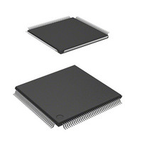
DF2166VT33WV Renesas Electronics America, DF2166VT33WV Datasheet - Page 481

DF2166VT33WV
Manufacturer Part Number
DF2166VT33WV
Description
MCU 16BIT FLASH 3V 512K 144-TQFP
Manufacturer
Renesas Electronics America
Series
H8® H8S/2100r
Datasheet
1.HS2168EPI61H-U.pdf
(876 pages)
Specifications of DF2166VT33WV
Core Processor
H8S/2000
Core Size
16-Bit
Speed
33MHz
Connectivity
I²C, IrDA, LPC, SCI, SmartCard
Peripherals
POR, PWM, WDT
Number Of I /o
106
Program Memory Size
512KB (512K x 8)
Program Memory Type
FLASH
Ram Size
40K x 8
Voltage - Supply (vcc/vdd)
3 V ~ 3.6 V
Data Converters
A/D 8x10b; D/A 2x8b
Oscillator Type
External
Operating Temperature
-20°C ~ 75°C
Package / Case
144-TQFP, 144-VQFP
Lead Free Status / RoHS Status
Lead free / RoHS Compliant
Eeprom Size
-
Available stocks
Company
Part Number
Manufacturer
Quantity
Price
Company:
Part Number:
DF2166VT33WV
Manufacturer:
Renesas Electronics America
Quantity:
135
Company:
Part Number:
DF2166VT33WV
Manufacturer:
Renesas Electronics America
Quantity:
10 000
- Current page: 481 of 876
- Download datasheet (5Mb)
15.3
The I
and SAR are allocated to the same addresses. Accessible registers differ depending on the ICE bit
in ICCR. When the ICE bit is cleared to 0, SAR and SARX can be accessed, and when the ICE bit
is set to 1, ICMR and ICDR can be accessed. The IIC registers are allocated to the same address.
Selecting register is carried out by means of the IICE bit in the serial timer control register
(STCR).
• I
• Slave address register (SAR)
• Second slave address register (SARX)
• I
• I
• I
• I
• I
• I
15.3.1
ICDR is an 8-bit readable/writable register that is used as a transmit data register when
transmitting and a receive data register when receiving. ICDR is divided internally into a shift
register (ICDRS), receive buffer (ICDRR), and transmit buffer (ICDRT). Data transfers among the
three registers are performed automatically in accordance with changes in the bus state, and they
affect the status of internal flags such as ICDRE and ICDRF.
In master transmit mode with the I
performed after start condition detection. When the start condition is detected, previous write data
is ignored. In slave transmit mode, writing should be performed after the slave addresses match
and the TRS bit is automatically changed to 1.
If IIC is in transmit mode (TRS=1) and the next data is in ICDRT (the ICDRE flag is 0), data is
transferred automatically from ICDRT to ICDRS, following transmission of one frame of data
using ICDRS. When the ICDRE flag is 1 and the next transmit data writing is waited, data is
transferred automatically from ICDRT to ICDRS by writing to ICDR. If IIC is in receive mode
(TRS=0), no data is transferred from ICDRT to ICDRS. Note that data should not be written to
ICDR in receive mode.
Reading receive data from ICDR is performed after data is transferred from ICDRS to ICDRR.
2
2
2
2
2
2
2
C bus data register (ICDR)
C bus mode register (ICMR)
C bus transfer rate select register (IICX3)
C bus control register (ICCR)
C bus status register (ICSR)
C bus extended control register (ICXR)
C SMbus control register (ICSMBCR)
2
C bus interface has the following registers. Registers ICDR and SARX and registers ICMR
Register Descriptions
I
2
C Bus Data Register (ICDR)
2
C bus format, writing transmit data to ICDR should be
Rev. 3.00, 03/04, page 439 of 830
Related parts for DF2166VT33WV
Image
Part Number
Description
Manufacturer
Datasheet
Request
R

Part Number:
Description:
KIT STARTER FOR M16C/29
Manufacturer:
Renesas Electronics America
Datasheet:

Part Number:
Description:
KIT STARTER FOR R8C/2D
Manufacturer:
Renesas Electronics America
Datasheet:

Part Number:
Description:
R0K33062P STARTER KIT
Manufacturer:
Renesas Electronics America
Datasheet:

Part Number:
Description:
KIT STARTER FOR R8C/23 E8A
Manufacturer:
Renesas Electronics America
Datasheet:

Part Number:
Description:
KIT STARTER FOR R8C/25
Manufacturer:
Renesas Electronics America
Datasheet:

Part Number:
Description:
KIT STARTER H8S2456 SHARPE DSPLY
Manufacturer:
Renesas Electronics America
Datasheet:

Part Number:
Description:
KIT STARTER FOR R8C38C
Manufacturer:
Renesas Electronics America
Datasheet:

Part Number:
Description:
KIT STARTER FOR R8C35C
Manufacturer:
Renesas Electronics America
Datasheet:

Part Number:
Description:
KIT STARTER FOR R8CL3AC+LCD APPS
Manufacturer:
Renesas Electronics America
Datasheet:

Part Number:
Description:
KIT STARTER FOR RX610
Manufacturer:
Renesas Electronics America
Datasheet:

Part Number:
Description:
KIT STARTER FOR R32C/118
Manufacturer:
Renesas Electronics America
Datasheet:

Part Number:
Description:
KIT DEV RSK-R8C/26-29
Manufacturer:
Renesas Electronics America
Datasheet:

Part Number:
Description:
KIT STARTER FOR SH7124
Manufacturer:
Renesas Electronics America
Datasheet:

Part Number:
Description:
KIT STARTER FOR H8SX/1622
Manufacturer:
Renesas Electronics America
Datasheet:

Part Number:
Description:
KIT DEV FOR SH7203
Manufacturer:
Renesas Electronics America
Datasheet:


