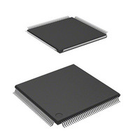
DF2166VT33WV Renesas Electronics America, DF2166VT33WV Datasheet - Page 271

DF2166VT33WV
Manufacturer Part Number
DF2166VT33WV
Description
MCU 16BIT FLASH 3V 512K 144-TQFP
Manufacturer
Renesas Electronics America
Series
H8® H8S/2100r
Datasheet
1.HS2168EPI61H-U.pdf
(876 pages)
Specifications of DF2166VT33WV
Core Processor
H8S/2000
Core Size
16-Bit
Speed
33MHz
Connectivity
I²C, IrDA, LPC, SCI, SmartCard
Peripherals
POR, PWM, WDT
Number Of I /o
106
Program Memory Size
512KB (512K x 8)
Program Memory Type
FLASH
Ram Size
40K x 8
Voltage - Supply (vcc/vdd)
3 V ~ 3.6 V
Data Converters
A/D 8x10b; D/A 2x8b
Oscillator Type
External
Operating Temperature
-20°C ~ 75°C
Package / Case
144-TQFP, 144-VQFP
Lead Free Status / RoHS Status
Lead free / RoHS Compliant
Eeprom Size
-
Available stocks
Company
Part Number
Manufacturer
Quantity
Price
Company:
Part Number:
DF2166VT33WV
Manufacturer:
Renesas Electronics America
Quantity:
135
Company:
Part Number:
DF2166VT33WV
Manufacturer:
Renesas Electronics America
Quantity:
10 000
- Current page: 271 of 876
- Download datasheet (5Mb)
• PA0 /KIN8/EVENT0/A16/SSE0I
Single-Chip Mode and Address-Data Multiplex Extended Mode: Port A functions as keyboard
input, external control input of SCI_0 and SCI_2, and also as an I/O port, and input or output can
be specified in bit units.
• PA7/KIN15/EVENT7, PA6/KIN14/EVENT6, PA5/KIN13/EVENT5, PA4/KIN12/EVENT4,
SSE
C/A
CEK1
PA1DDR
Address 13
Pin function
SSE
C/A
CKE1
PA0DDR
Address 13
Pin function
The function of port A pins is switched as shown below according to the combination of the
SSE bit in SEMR of SCI_0, the C/A bit in SMR, the CKE1 bit in SCR, address 13 setting, and
the PA0DDR bit.
When the KMIM8 bit in KMIMRA of the interrupt controller is cleared to 0, this pin can be
used as the KIN8 input pin. To use this pin as the KIN8 input pin, clear the PA0DDR bit to 0.
When this pin is used as EVENT0 input pin according to bits ECSB3 to ECSB0 in ECCR of
the data transfer controller settings, clear the PA0DDR bit to 0. Though this pin has been set to
the EVENT0 input pin, to use as the PA0 or A16 output pin, set the PA0DDR bit to 1.
PA3/KIN11/EVENT3, PA2/KIN10/EVENT2
When the KMIM bit in KMIMRA of the interrupt controller is cleared to 0, this pin can be
used as the KIN input pin. To use this pin as the KIN input pin, clear the PAnDDR bit to 0.
When this pin is used as the EVENT input pin according to bits ECSB3 to ECSB0 in ECCR of
the data transfer controller settings, clear the PAnDDR bit to 0. Though this pin has been set to
the EVENT input pin, to use as the PAn output pins, set the PAnDDR bit to 1.
/EVENT1 input pin
KIN9 input pin
/EVENT0 input pin
PA1 input pin
KIN8 input pin
PA0 input pin
0
0
1
1
PA1 output pin
PA0 output pin
0
1
1
0
A17 output pin
A16 output pin
1
0
Rev. 3.00, 03/04, page 229 of 830
1
0
SSE2I input pin
SSE0I input pin
1
1
1
1
1
1
Related parts for DF2166VT33WV
Image
Part Number
Description
Manufacturer
Datasheet
Request
R

Part Number:
Description:
KIT STARTER FOR M16C/29
Manufacturer:
Renesas Electronics America
Datasheet:

Part Number:
Description:
KIT STARTER FOR R8C/2D
Manufacturer:
Renesas Electronics America
Datasheet:

Part Number:
Description:
R0K33062P STARTER KIT
Manufacturer:
Renesas Electronics America
Datasheet:

Part Number:
Description:
KIT STARTER FOR R8C/23 E8A
Manufacturer:
Renesas Electronics America
Datasheet:

Part Number:
Description:
KIT STARTER FOR R8C/25
Manufacturer:
Renesas Electronics America
Datasheet:

Part Number:
Description:
KIT STARTER H8S2456 SHARPE DSPLY
Manufacturer:
Renesas Electronics America
Datasheet:

Part Number:
Description:
KIT STARTER FOR R8C38C
Manufacturer:
Renesas Electronics America
Datasheet:

Part Number:
Description:
KIT STARTER FOR R8C35C
Manufacturer:
Renesas Electronics America
Datasheet:

Part Number:
Description:
KIT STARTER FOR R8CL3AC+LCD APPS
Manufacturer:
Renesas Electronics America
Datasheet:

Part Number:
Description:
KIT STARTER FOR RX610
Manufacturer:
Renesas Electronics America
Datasheet:

Part Number:
Description:
KIT STARTER FOR R32C/118
Manufacturer:
Renesas Electronics America
Datasheet:

Part Number:
Description:
KIT DEV RSK-R8C/26-29
Manufacturer:
Renesas Electronics America
Datasheet:

Part Number:
Description:
KIT STARTER FOR SH7124
Manufacturer:
Renesas Electronics America
Datasheet:

Part Number:
Description:
KIT STARTER FOR H8SX/1622
Manufacturer:
Renesas Electronics America
Datasheet:

Part Number:
Description:
KIT DEV FOR SH7203
Manufacturer:
Renesas Electronics America
Datasheet:


