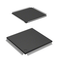
DF2166VT33WV Renesas Electronics America, DF2166VT33WV Datasheet - Page 356

DF2166VT33WV
Manufacturer Part Number
DF2166VT33WV
Description
MCU 16BIT FLASH 3V 512K 144-TQFP
Manufacturer
Renesas Electronics America
Series
H8® H8S/2100r
Datasheet
1.HS2168EPI61H-U.pdf
(876 pages)
Specifications of DF2166VT33WV
Core Processor
H8S/2000
Core Size
16-Bit
Speed
33MHz
Connectivity
I²C, IrDA, LPC, SCI, SmartCard
Peripherals
POR, PWM, WDT
Number Of I /o
106
Program Memory Size
512KB (512K x 8)
Program Memory Type
FLASH
Ram Size
40K x 8
Voltage - Supply (vcc/vdd)
3 V ~ 3.6 V
Data Converters
A/D 8x10b; D/A 2x8b
Oscillator Type
External
Operating Temperature
-20°C ~ 75°C
Package / Case
144-TQFP, 144-VQFP
Lead Free Status / RoHS Status
Lead free / RoHS Compliant
Eeprom Size
-
Available stocks
Company
Part Number
Manufacturer
Quantity
Price
Company:
Part Number:
DF2166VT33WV
Manufacturer:
Renesas Electronics America
Quantity:
135
Company:
Part Number:
DF2166VT33WV
Manufacturer:
Renesas Electronics America
Quantity:
10 000
- Current page: 356 of 876
- Download datasheet (5Mb)
12.3.5
TCSR indicates the status flags and controls compare-match output. About the TCSR_Y and
TCSR_X accesses see section 3.2.2, System Control Register (SYSCR).
• TCSR_0
Rev. 3.00, 03/04, page 314 of 830
Bit
7
6
5
4
3
2
Timer Control/Status Register (TCSR)
Bit Name Initial Value R/W
OS3
OS2
CMFB
CMFA
OVF
ADTE
0
0
0
0
0
0
R/(W)* Compare-Match Flag B
R/(W)* Compare-Match Flag A
R/(W)* Timer Overflow Flag
R/W
R/W
R/W
Description
[Setting condition]
When the values of TCNT_0 and TCORB_0 match
[Clearing condition]
Read CMFB when CMFB = 1, then write 0 in CMFB
[Setting condition]
When the values of TCNT_0 and TCORA_0 match
[Clearing condition]
Read CMFA when CMFA = 1, then write 0 in CMFA
[Setting condition]
When TCNT_0 overflows from H′FF to H′00
[Clearing condition]
Read OVF when OVF = 1, then write 0 in OVF
A/D Trigger Enable
Enables or disables A/D converter start requests by
compare-match A.
0: A/D converter start requests by compare-match A
1: A/D converter start requests by compare-match A
Output Select 3 and 2
These bits specify how the TMO0 pin output level is
to be changed by compare-match B of TCORB_0
and TCNT_0.
00: No change
01: 0 is output
10: 1 is output
11: Output is inverted (toggle output)
are disabled
are enabled
Related parts for DF2166VT33WV
Image
Part Number
Description
Manufacturer
Datasheet
Request
R

Part Number:
Description:
KIT STARTER FOR M16C/29
Manufacturer:
Renesas Electronics America
Datasheet:

Part Number:
Description:
KIT STARTER FOR R8C/2D
Manufacturer:
Renesas Electronics America
Datasheet:

Part Number:
Description:
R0K33062P STARTER KIT
Manufacturer:
Renesas Electronics America
Datasheet:

Part Number:
Description:
KIT STARTER FOR R8C/23 E8A
Manufacturer:
Renesas Electronics America
Datasheet:

Part Number:
Description:
KIT STARTER FOR R8C/25
Manufacturer:
Renesas Electronics America
Datasheet:

Part Number:
Description:
KIT STARTER H8S2456 SHARPE DSPLY
Manufacturer:
Renesas Electronics America
Datasheet:

Part Number:
Description:
KIT STARTER FOR R8C38C
Manufacturer:
Renesas Electronics America
Datasheet:

Part Number:
Description:
KIT STARTER FOR R8C35C
Manufacturer:
Renesas Electronics America
Datasheet:

Part Number:
Description:
KIT STARTER FOR R8CL3AC+LCD APPS
Manufacturer:
Renesas Electronics America
Datasheet:

Part Number:
Description:
KIT STARTER FOR RX610
Manufacturer:
Renesas Electronics America
Datasheet:

Part Number:
Description:
KIT STARTER FOR R32C/118
Manufacturer:
Renesas Electronics America
Datasheet:

Part Number:
Description:
KIT DEV RSK-R8C/26-29
Manufacturer:
Renesas Electronics America
Datasheet:

Part Number:
Description:
KIT STARTER FOR SH7124
Manufacturer:
Renesas Electronics America
Datasheet:

Part Number:
Description:
KIT STARTER FOR H8SX/1622
Manufacturer:
Renesas Electronics America
Datasheet:

Part Number:
Description:
KIT DEV FOR SH7203
Manufacturer:
Renesas Electronics America
Datasheet:


