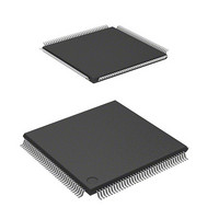
DF2166VT33WV Renesas Electronics America, DF2166VT33WV Datasheet - Page 29

DF2166VT33WV
Manufacturer Part Number
DF2166VT33WV
Description
MCU 16BIT FLASH 3V 512K 144-TQFP
Manufacturer
Renesas Electronics America
Series
H8® H8S/2100r
Datasheet
1.HS2168EPI61H-U.pdf
(876 pages)
Specifications of DF2166VT33WV
Core Processor
H8S/2000
Core Size
16-Bit
Speed
33MHz
Connectivity
I²C, IrDA, LPC, SCI, SmartCard
Peripherals
POR, PWM, WDT
Number Of I /o
106
Program Memory Size
512KB (512K x 8)
Program Memory Type
FLASH
Ram Size
40K x 8
Voltage - Supply (vcc/vdd)
3 V ~ 3.6 V
Data Converters
A/D 8x10b; D/A 2x8b
Oscillator Type
External
Operating Temperature
-20°C ~ 75°C
Package / Case
144-TQFP, 144-VQFP
Lead Free Status / RoHS Status
Lead free / RoHS Compliant
Eeprom Size
-
Available stocks
Company
Part Number
Manufacturer
Quantity
Price
Company:
Part Number:
DF2166VT33WV
Manufacturer:
Renesas Electronics America
Quantity:
135
Company:
Part Number:
DF2166VT33WV
Manufacturer:
Renesas Electronics America
Quantity:
10 000
- Current page: 29 of 876
- Download datasheet (5Mb)
Figure 7.11 DTC Operation Timing (Example of Chain Transfer) ............................................ 171
Section 8 I/O Ports
Figure 8.1 Noise Canceler Circuit .............................................................................................. 208
Figure 8.2 Noise Canceler Operation.......................................................................................... 208
Section 9 8-Bit PWM Timer (PWM)
Figure 9.1 Block Diagram of PWM Timer ................................................................................. 251
Figure 9.2 Example of Additional Pulse Timing (When Upper 4 Bits of PWDR = B'1000) ..... 259
Figure 9.3 Example of PWM Setting.......................................................................................... 260
Figure 9.4 Example when PWM is Used as D/A Converter....................................................... 260
Section 10 14-Bit PWM Timer (PWMX)
Figure 10.1 PWMX (D/A) Block Diagram................................................................................. 261
Figure 10.2 PWMX (D/A) Operation ......................................................................................... 269
Figure 10.3 Output Waveform (OS = 0, DADR corresponds to T
Figure 10.4 Output Waveform (OS = 1, DADR corresponds to T
Figure 10.5 D/A Data Register Configuration when CFS = 1 .................................................... 273
Figure 10.6 Output Waveform when DADR = H'0207 (OS = 1) ............................................... 274
Section 11 16-Bit Free-Running Timer (FRT)
Figure 11.1 Block Diagram of 16-Bit Free-Running Timer ....................................................... 278
Figure 11.2 Example of Pulse Output......................................................................................... 289
Figure 11.3 Increment Timing with Internal Clock Source ........................................................ 290
Figure 11.4 Increment Timing with External Clock Source ....................................................... 290
Figure 11.5 Timing of Output Compare A Output ..................................................................... 291
Figure 11.6 Clearing of FRC by Compare-Match A Signal ....................................................... 291
Figure 11.7 Input Capture Input Signal Timing (Usual Case) .................................................... 292
Figure 11.8 Input Capture Input Signal Timing (When ICRA to ICRD is Read)....................... 292
Figure 11.9 Buffered Input Capture Timing ............................................................................... 293
Figure 11.10 Buffered Input Capture Timing (BUFEA = 1) ...................................................... 294
Figure 11.11 Timing of Input Capture Flag (ICFA to ICFD) Setting......................................... 294
Figure 11.12 Timing of Output Compare Flag (OCFA or OCFB) Setting ................................. 295
Figure 11.13 Timing of Overflow Flag (OVF) Setting............................................................... 295
Figure 11.14 OCRA Automatic Addition Timing ...................................................................... 296
Figure 11.15 Timing of Input Capture Mask Signal Setting....................................................... 296
Figure 11.16 Timing of Input Capture Mask Signal Clearing .................................................... 297
Figure 11.17 Conflict between FRC Write and Clear................................................................. 299
Figure 11.18 Conflict between FRC Write and Increment ......................................................... 300
Figure 11.19 Conflict between OCR Write and Compare-Match
Figure 11.20 Conflict between OCR Write and Compare-Match
(When Automatic Addition Function is Not Used)............................................... 301
(When Automatic Addition Function is Used)...................................................... 302
L
H
Rev. 3.00, 03/04, page xxvii of xl
) .......................................... 272
) .......................................... 273
Related parts for DF2166VT33WV
Image
Part Number
Description
Manufacturer
Datasheet
Request
R

Part Number:
Description:
KIT STARTER FOR M16C/29
Manufacturer:
Renesas Electronics America
Datasheet:

Part Number:
Description:
KIT STARTER FOR R8C/2D
Manufacturer:
Renesas Electronics America
Datasheet:

Part Number:
Description:
R0K33062P STARTER KIT
Manufacturer:
Renesas Electronics America
Datasheet:

Part Number:
Description:
KIT STARTER FOR R8C/23 E8A
Manufacturer:
Renesas Electronics America
Datasheet:

Part Number:
Description:
KIT STARTER FOR R8C/25
Manufacturer:
Renesas Electronics America
Datasheet:

Part Number:
Description:
KIT STARTER H8S2456 SHARPE DSPLY
Manufacturer:
Renesas Electronics America
Datasheet:

Part Number:
Description:
KIT STARTER FOR R8C38C
Manufacturer:
Renesas Electronics America
Datasheet:

Part Number:
Description:
KIT STARTER FOR R8C35C
Manufacturer:
Renesas Electronics America
Datasheet:

Part Number:
Description:
KIT STARTER FOR R8CL3AC+LCD APPS
Manufacturer:
Renesas Electronics America
Datasheet:

Part Number:
Description:
KIT STARTER FOR RX610
Manufacturer:
Renesas Electronics America
Datasheet:

Part Number:
Description:
KIT STARTER FOR R32C/118
Manufacturer:
Renesas Electronics America
Datasheet:

Part Number:
Description:
KIT DEV RSK-R8C/26-29
Manufacturer:
Renesas Electronics America
Datasheet:

Part Number:
Description:
KIT STARTER FOR SH7124
Manufacturer:
Renesas Electronics America
Datasheet:

Part Number:
Description:
KIT STARTER FOR H8SX/1622
Manufacturer:
Renesas Electronics America
Datasheet:

Part Number:
Description:
KIT DEV FOR SH7203
Manufacturer:
Renesas Electronics America
Datasheet:


