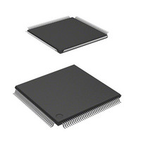
DF2166VT33WV Renesas Electronics America, DF2166VT33WV Datasheet - Page 828

DF2166VT33WV
Manufacturer Part Number
DF2166VT33WV
Description
MCU 16BIT FLASH 3V 512K 144-TQFP
Manufacturer
Renesas Electronics America
Series
H8® H8S/2100r
Datasheet
1.HS2168EPI61H-U.pdf
(876 pages)
Specifications of DF2166VT33WV
Core Processor
H8S/2000
Core Size
16-Bit
Speed
33MHz
Connectivity
I²C, IrDA, LPC, SCI, SmartCard
Peripherals
POR, PWM, WDT
Number Of I /o
106
Program Memory Size
512KB (512K x 8)
Program Memory Type
FLASH
Ram Size
40K x 8
Voltage - Supply (vcc/vdd)
3 V ~ 3.6 V
Data Converters
A/D 8x10b; D/A 2x8b
Oscillator Type
External
Operating Temperature
-20°C ~ 75°C
Package / Case
144-TQFP, 144-VQFP
Lead Free Status / RoHS Status
Lead free / RoHS Compliant
Eeprom Size
-
Available stocks
Company
Part Number
Manufacturer
Quantity
Price
Company:
Part Number:
DF2166VT33WV
Manufacturer:
Renesas Electronics America
Quantity:
135
Company:
Part Number:
DF2166VT33WV
Manufacturer:
Renesas Electronics America
Quantity:
10 000
- Current page: 828 of 876
- Download datasheet (5Mb)
Notes:
Rev. 3.00, 03/04, page 786 of 830
Item
Analog
power
supply
current
Reference
power
supply
current
Input
capacitance
RAM standby voltage
VCC start voltage
VCC rising edge
1. Do not leave the AVCC, AVref, and AVSS pins open even if the A/D converter or D/A converter is
2. When noise cancel has been enabled.
3. An external pull-up resistor is necessary to provide high-level output from SCL5 to SCL0 and
4. Port 8, C0 to C5, D6, and D7 are NMOS push-pull outputs.
5. Current consumption values are for V
6. When VCC = 3.0 V, V
not used.
Even if the A/D converter or D/A converter is not used, apply a value in the range from 3.0 V to 3.6
V to the AVCC and AVref pins by connecting them to the power supply (VCC). The relationship
between these two pins should be AVref ≤ AVCC.
SDA5 to SDA0 (ICE bit in ICCR is 1).
Port 8, C0 to C5, D6, D7, and SCK0 to SCK2 (ICE bit in ICCR = 0) high levels are driven by
NMOS. An external pull-up resistor is necessary to provide high-level output from these pins when
they are used as an output.
unloaded and the on-chip pull-up MOSs in the off state.
During A/D, D/A conversion
A/D, D/A conversion
standby
During A/D conversion
During A/D, D/A conversion
A/D, D/A conversion
standby
All input pin
IH
min = VCC – 0.2 V, and V
Symbol Min. Typ. Max. Unit
AI
AI
C
V
VCC
SVCC
RAM
in
cc
ref
START
IH
min = VCC – 0.2 V and V
3.0
1.0
2.5
0.1
0.5
0.5
0
IL
max = 0.2 V.
5.0
5.0
5.0
10
0.8
20
2.0
1.0
mA
µA
mA
µA
pF
V
V
ms/V
IL
max = 0.2 V with all output pins
Test
Conditions
V
T
a
in
= 25 °C
= 0 V, f = 1 MHz,
Related parts for DF2166VT33WV
Image
Part Number
Description
Manufacturer
Datasheet
Request
R

Part Number:
Description:
KIT STARTER FOR M16C/29
Manufacturer:
Renesas Electronics America
Datasheet:

Part Number:
Description:
KIT STARTER FOR R8C/2D
Manufacturer:
Renesas Electronics America
Datasheet:

Part Number:
Description:
R0K33062P STARTER KIT
Manufacturer:
Renesas Electronics America
Datasheet:

Part Number:
Description:
KIT STARTER FOR R8C/23 E8A
Manufacturer:
Renesas Electronics America
Datasheet:

Part Number:
Description:
KIT STARTER FOR R8C/25
Manufacturer:
Renesas Electronics America
Datasheet:

Part Number:
Description:
KIT STARTER H8S2456 SHARPE DSPLY
Manufacturer:
Renesas Electronics America
Datasheet:

Part Number:
Description:
KIT STARTER FOR R8C38C
Manufacturer:
Renesas Electronics America
Datasheet:

Part Number:
Description:
KIT STARTER FOR R8C35C
Manufacturer:
Renesas Electronics America
Datasheet:

Part Number:
Description:
KIT STARTER FOR R8CL3AC+LCD APPS
Manufacturer:
Renesas Electronics America
Datasheet:

Part Number:
Description:
KIT STARTER FOR RX610
Manufacturer:
Renesas Electronics America
Datasheet:

Part Number:
Description:
KIT STARTER FOR R32C/118
Manufacturer:
Renesas Electronics America
Datasheet:

Part Number:
Description:
KIT DEV RSK-R8C/26-29
Manufacturer:
Renesas Electronics America
Datasheet:

Part Number:
Description:
KIT STARTER FOR SH7124
Manufacturer:
Renesas Electronics America
Datasheet:

Part Number:
Description:
KIT STARTER FOR H8SX/1622
Manufacturer:
Renesas Electronics America
Datasheet:

Part Number:
Description:
KIT DEV FOR SH7203
Manufacturer:
Renesas Electronics America
Datasheet:


