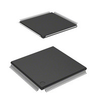
DF2166VT33WV Renesas Electronics America, DF2166VT33WV Datasheet - Page 616

DF2166VT33WV
Manufacturer Part Number
DF2166VT33WV
Description
MCU 16BIT FLASH 3V 512K 144-TQFP
Manufacturer
Renesas Electronics America
Series
H8® H8S/2100r
Datasheet
1.HS2168EPI61H-U.pdf
(876 pages)
Specifications of DF2166VT33WV
Core Processor
H8S/2000
Core Size
16-Bit
Speed
33MHz
Connectivity
I²C, IrDA, LPC, SCI, SmartCard
Peripherals
POR, PWM, WDT
Number Of I /o
106
Program Memory Size
512KB (512K x 8)
Program Memory Type
FLASH
Ram Size
40K x 8
Voltage - Supply (vcc/vdd)
3 V ~ 3.6 V
Data Converters
A/D 8x10b; D/A 2x8b
Oscillator Type
External
Operating Temperature
-20°C ~ 75°C
Package / Case
144-TQFP, 144-VQFP
Lead Free Status / RoHS Status
Lead free / RoHS Compliant
Eeprom Size
-
Available stocks
Company
Part Number
Manufacturer
Quantity
Price
Company:
Part Number:
DF2166VT33WV
Manufacturer:
Renesas Electronics America
Quantity:
135
Company:
Part Number:
DF2166VT33WV
Manufacturer:
Renesas Electronics America
Quantity:
10 000
- Current page: 616 of 876
- Download datasheet (5Mb)
16.4.5
The A20 gate signal can mask address A20 to emulate an addressing mode used by personal
computers with an 8086-family CPU*. A regular-speed A20 gate signal can be output under
firmware control. The fast A20 gate function that is speeded up by the hardware is enabled by
setting the FGA20E bit to 1 in HICR0.
Note: * An Intel microcomputer
Regular A20 Gate Operation: Output of the A20 gate signal can be controlled by an H'D1
command followed by data. When the slave processor (this LSI) receives data, it normally uses an
interrupt routine activated by the IBFI1 interrupt to read IDR1. If the data follows an H'D1
command, firmware copies bit 1 of the data and outputs it at the gate A20 pin.
Fast A20 Gate Operation: The internal state of GA20 output is initialized to 1 when FGA20E =
0. When the FGA20E bit is set to 1, PD3/GA20 is used for output of a fast A20 gate signal. The
state of the PD3/GA20 pin can be monitored by reading the GA20 bit in HICR2.
The initial output from this pin will be a logic 1, which is the initial value. Afterward, the host
processor can manipulate the output from this pin by sending commands and data. This function is
only available via the IDR1 register. The LPC interface decodes commands input from the host.
When an H'D1 host command is detected, bit 1 of the data following the host command is output
from the GA20 output pin. This operation does not depend on firmware or interrupts, and is faster
than the regular processing using interrupts. Table 16.6 shows the conditions that set and clear
GA20 (PD3). Figure 16.8 shows the GA20 output in flowchart form. Table 16.7 indicates the
GA20 output signal values.
Table 16.6 GA20 (PD3) Set/Clear Conditions
Rev. 3.00, 03/04, page 574 of 830
Pin Name
GA20 (PD3)
A20 Gate
Setting Condition
When bit 1 of the data that follows an
H'D1 host command is 1
Clearing Condition
When bit 1 of the data follows an H'D1
host command is 0
Related parts for DF2166VT33WV
Image
Part Number
Description
Manufacturer
Datasheet
Request
R

Part Number:
Description:
KIT STARTER FOR M16C/29
Manufacturer:
Renesas Electronics America
Datasheet:

Part Number:
Description:
KIT STARTER FOR R8C/2D
Manufacturer:
Renesas Electronics America
Datasheet:

Part Number:
Description:
R0K33062P STARTER KIT
Manufacturer:
Renesas Electronics America
Datasheet:

Part Number:
Description:
KIT STARTER FOR R8C/23 E8A
Manufacturer:
Renesas Electronics America
Datasheet:

Part Number:
Description:
KIT STARTER FOR R8C/25
Manufacturer:
Renesas Electronics America
Datasheet:

Part Number:
Description:
KIT STARTER H8S2456 SHARPE DSPLY
Manufacturer:
Renesas Electronics America
Datasheet:

Part Number:
Description:
KIT STARTER FOR R8C38C
Manufacturer:
Renesas Electronics America
Datasheet:

Part Number:
Description:
KIT STARTER FOR R8C35C
Manufacturer:
Renesas Electronics America
Datasheet:

Part Number:
Description:
KIT STARTER FOR R8CL3AC+LCD APPS
Manufacturer:
Renesas Electronics America
Datasheet:

Part Number:
Description:
KIT STARTER FOR RX610
Manufacturer:
Renesas Electronics America
Datasheet:

Part Number:
Description:
KIT STARTER FOR R32C/118
Manufacturer:
Renesas Electronics America
Datasheet:

Part Number:
Description:
KIT DEV RSK-R8C/26-29
Manufacturer:
Renesas Electronics America
Datasheet:

Part Number:
Description:
KIT STARTER FOR SH7124
Manufacturer:
Renesas Electronics America
Datasheet:

Part Number:
Description:
KIT STARTER FOR H8SX/1622
Manufacturer:
Renesas Electronics America
Datasheet:

Part Number:
Description:
KIT DEV FOR SH7203
Manufacturer:
Renesas Electronics America
Datasheet:


