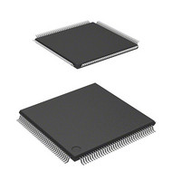
DF2166VT33WV Renesas Electronics America, DF2166VT33WV Datasheet - Page 538

DF2166VT33WV
Manufacturer Part Number
DF2166VT33WV
Description
MCU 16BIT FLASH 3V 512K 144-TQFP
Manufacturer
Renesas Electronics America
Series
H8® H8S/2100r
Datasheet
1.HS2168EPI61H-U.pdf
(876 pages)
Specifications of DF2166VT33WV
Core Processor
H8S/2000
Core Size
16-Bit
Speed
33MHz
Connectivity
I²C, IrDA, LPC, SCI, SmartCard
Peripherals
POR, PWM, WDT
Number Of I /o
106
Program Memory Size
512KB (512K x 8)
Program Memory Type
FLASH
Ram Size
40K x 8
Voltage - Supply (vcc/vdd)
3 V ~ 3.6 V
Data Converters
A/D 8x10b; D/A 2x8b
Oscillator Type
External
Operating Temperature
-20°C ~ 75°C
Package / Case
144-TQFP, 144-VQFP
Lead Free Status / RoHS Status
Lead free / RoHS Compliant
Eeprom Size
-
Available stocks
Company
Part Number
Manufacturer
Quantity
Price
Company:
Part Number:
DF2166VT33WV
Manufacturer:
Renesas Electronics America
Quantity:
135
Company:
Part Number:
DF2166VT33WV
Manufacturer:
Renesas Electronics America
Quantity:
10 000
- Current page: 538 of 876
- Download datasheet (5Mb)
4. SCL and SDA input is sampled in synchronization with the internal clock. The AC timing
5. The I
Table 15.12 Permissible SCL Rise Time (t
TCSS IICXn
0
1
1
Note: n = 0 to 5
6. The I
Rev. 3.00, 03/04, page 496 of 830
therefore depends on the system clock cycle t
Characteristics. Note that the I
system clock frequency of less than 5 MHz.
speed mode). In master mode, the I
one bit at a time during communication. If t
the time determined by the input clock of the I
extended. The SCL rise time is determined by the pull-up resistance and load capacitance of
the SCL line. To insure proper operation at the set transfer rate, adjust the pull-up resistance
and load capacitance so that the SCL rise time does not exceed the values given in table 15.12.
and 300 ns. The I
table 15.11. However, because of the rise and fall times, the I
may not be satisfied at the maximum transfer rate. Table 15.13 shows output timing
calculations for different operating frequencies, including the worst-case influence of rise and
fall times.
0
1
0
1
2
2
C bus interface specification for the SCL rise time t
C bus interface specifications for the SCL and SDA rise and fall times are under 1000 ns
t
Indi-
cation
7.5 t
17.5 t
37.5 t
cyc
cyc
2
cyc
cyc
C bus interface SCL and SDA output timing is prescribed by t
Standard
mode
High-
speed
mode
Standard
mode
High-
speed
mode
Standard
mode
High-
speed
mode
I
Spe-
cifica-
tion
(Max.)
1000
300
1000
300
1000
300
2
2
C bus interface AC timing specification will not be met with a
C Bus
2
C bus interface monitors the SCL line and synchronizes
φ = 5
MHz
1000
300
1000
300
1000
300
sr
) Values
sr
(the time for SCL to go from low to V
cyc
2
C bus interface, the high period of SCL is
, as shown in section 25, Electrical
φ = 8
MHz
937
300
1000
300
1000
300
Time Indication [ns]
φ = 10
MHz
750
300
1000
300
1000
300
sr
is 1000 ns or less (300 ns for high-
2
C bus interface specifications
φ = 16
MHz
468
300
1000
300
1000
300
φ = 20
MHz
375
300
875
300
1000
300
cyc
φ = 25
MHz
300
300
700
300
1000
300
, as shown in
IH
) exceeds
φ = 33
MHz
227
227
530
300
1000
300
Related parts for DF2166VT33WV
Image
Part Number
Description
Manufacturer
Datasheet
Request
R

Part Number:
Description:
KIT STARTER FOR M16C/29
Manufacturer:
Renesas Electronics America
Datasheet:

Part Number:
Description:
KIT STARTER FOR R8C/2D
Manufacturer:
Renesas Electronics America
Datasheet:

Part Number:
Description:
R0K33062P STARTER KIT
Manufacturer:
Renesas Electronics America
Datasheet:

Part Number:
Description:
KIT STARTER FOR R8C/23 E8A
Manufacturer:
Renesas Electronics America
Datasheet:

Part Number:
Description:
KIT STARTER FOR R8C/25
Manufacturer:
Renesas Electronics America
Datasheet:

Part Number:
Description:
KIT STARTER H8S2456 SHARPE DSPLY
Manufacturer:
Renesas Electronics America
Datasheet:

Part Number:
Description:
KIT STARTER FOR R8C38C
Manufacturer:
Renesas Electronics America
Datasheet:

Part Number:
Description:
KIT STARTER FOR R8C35C
Manufacturer:
Renesas Electronics America
Datasheet:

Part Number:
Description:
KIT STARTER FOR R8CL3AC+LCD APPS
Manufacturer:
Renesas Electronics America
Datasheet:

Part Number:
Description:
KIT STARTER FOR RX610
Manufacturer:
Renesas Electronics America
Datasheet:

Part Number:
Description:
KIT STARTER FOR R32C/118
Manufacturer:
Renesas Electronics America
Datasheet:

Part Number:
Description:
KIT DEV RSK-R8C/26-29
Manufacturer:
Renesas Electronics America
Datasheet:

Part Number:
Description:
KIT STARTER FOR SH7124
Manufacturer:
Renesas Electronics America
Datasheet:

Part Number:
Description:
KIT STARTER FOR H8SX/1622
Manufacturer:
Renesas Electronics America
Datasheet:

Part Number:
Description:
KIT DEV FOR SH7203
Manufacturer:
Renesas Electronics America
Datasheet:


