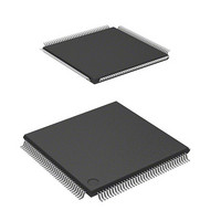
DF2166VT33WV Renesas Electronics America, DF2166VT33WV Datasheet - Page 8

DF2166VT33WV
Manufacturer Part Number
DF2166VT33WV
Description
MCU 16BIT FLASH 3V 512K 144-TQFP
Manufacturer
Renesas Electronics America
Series
H8® H8S/2100r
Datasheet
1.HS2168EPI61H-U.pdf
(876 pages)
Specifications of DF2166VT33WV
Core Processor
H8S/2000
Core Size
16-Bit
Speed
33MHz
Connectivity
I²C, IrDA, LPC, SCI, SmartCard
Peripherals
POR, PWM, WDT
Number Of I /o
106
Program Memory Size
512KB (512K x 8)
Program Memory Type
FLASH
Ram Size
40K x 8
Voltage - Supply (vcc/vdd)
3 V ~ 3.6 V
Data Converters
A/D 8x10b; D/A 2x8b
Oscillator Type
External
Operating Temperature
-20°C ~ 75°C
Package / Case
144-TQFP, 144-VQFP
Lead Free Status / RoHS Status
Lead free / RoHS Compliant
Eeprom Size
-
Available stocks
Company
Part Number
Manufacturer
Quantity
Price
Company:
Part Number:
DF2166VT33WV
Manufacturer:
Renesas Electronics America
Quantity:
135
Company:
Part Number:
DF2166VT33WV
Manufacturer:
Renesas Electronics America
Quantity:
10 000
- Current page: 8 of 876
- Download datasheet (5Mb)
This LSI is a microcomputer (MCU) made up of the H8S/2000 CPU with Renesas Technology's
original architecture as its core, and the peripheral functions required to configure a system, eg PC
server.
The H8S/2000 CPU has an internal 32-bit configuration, sixteen 16-bit general registers, and a
simple and optimized instruction set for high-speed operation. The H8S/2000 CPU can handle a
16-Mbyte linear address space. The instruction set of the H8S/2000 CPU maintains upward
compatibility at the object level with the H8/300 and H8/300H CPUs. This allows the transition
from the H8/300, H8/300L, or H8/300H to the H8S/2000 CPU.
This LSI is equipped with ROM, RAM, two kinds of PWM timers (PWM and PWMX), a 16-bit
free running timer (FRT), an 8-bit timer (TMR), a watchdog timer (WDT), a serial communication
interface (SCI), an I
converter, and I/O ports as on-chip peripheral modules required for system configuration.
A data transfer controller (DTC) is included as a bus master.
A flash memory (F-ZTAT
The CPU and ROM are connected to a 16-bit bus, enabling byte data and word data to be accessed
in a single state. This improves the instruction fetch and process speeds.
Two operating modes are provided, offering a choice of address space and single chip
mode/external extended mode. Boot programming into a flash memory, on-chip emulation, and
boundary scan can be selected as special operating modes.
Note: * F-ZTAT
Target Users: This manual was written for users who use this LSI in the design of application
Objective:
Notes on reading this manual:
• In order to understand the overall functions of the chip
Rev. 3.00, 03/04, page vi of xl
Read this manual in the order of the table of contents. This manual can be roughly categorized
into the descriptions on the CPU, system control functions, peripheral functions and electrical
characteristics.
systems. Target users are expected to understand the fundamentals of electrical
circuits, logic circuits, and microcomputers.
This manual was written to explain the hardware functions and electrical
characteristics of this LSI to the target users.
Refer to the H8S/2600 Series, H8S/2000 Series Programming Manual for a
detailed description of the instruction set.
TM
2
C bus interface (IIC), an LPC interface (LPC), a D/A converter, an A/D
is a trademark of Renesas Technology Corp.
TM
*) version is available for this LSI’s 256, 384, and 512-kbyte ROM.
Preface
Related parts for DF2166VT33WV
Image
Part Number
Description
Manufacturer
Datasheet
Request
R

Part Number:
Description:
KIT STARTER FOR M16C/29
Manufacturer:
Renesas Electronics America
Datasheet:

Part Number:
Description:
KIT STARTER FOR R8C/2D
Manufacturer:
Renesas Electronics America
Datasheet:

Part Number:
Description:
R0K33062P STARTER KIT
Manufacturer:
Renesas Electronics America
Datasheet:

Part Number:
Description:
KIT STARTER FOR R8C/23 E8A
Manufacturer:
Renesas Electronics America
Datasheet:

Part Number:
Description:
KIT STARTER FOR R8C/25
Manufacturer:
Renesas Electronics America
Datasheet:

Part Number:
Description:
KIT STARTER H8S2456 SHARPE DSPLY
Manufacturer:
Renesas Electronics America
Datasheet:

Part Number:
Description:
KIT STARTER FOR R8C38C
Manufacturer:
Renesas Electronics America
Datasheet:

Part Number:
Description:
KIT STARTER FOR R8C35C
Manufacturer:
Renesas Electronics America
Datasheet:

Part Number:
Description:
KIT STARTER FOR R8CL3AC+LCD APPS
Manufacturer:
Renesas Electronics America
Datasheet:

Part Number:
Description:
KIT STARTER FOR RX610
Manufacturer:
Renesas Electronics America
Datasheet:

Part Number:
Description:
KIT STARTER FOR R32C/118
Manufacturer:
Renesas Electronics America
Datasheet:

Part Number:
Description:
KIT DEV RSK-R8C/26-29
Manufacturer:
Renesas Electronics America
Datasheet:

Part Number:
Description:
KIT STARTER FOR SH7124
Manufacturer:
Renesas Electronics America
Datasheet:

Part Number:
Description:
KIT STARTER FOR H8SX/1622
Manufacturer:
Renesas Electronics America
Datasheet:

Part Number:
Description:
KIT DEV FOR SH7203
Manufacturer:
Renesas Electronics America
Datasheet:


