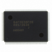
HD64F2638F20J Renesas Electronics America, HD64F2638F20J Datasheet - Page 297

HD64F2638F20J
Manufacturer Part Number
HD64F2638F20J
Description
IC H8S MCU FLASH 256K 128-QFP
Manufacturer
Renesas Electronics America
Series
H8® H8S/2600r
Specifications of HD64F2638F20J
Core Processor
H8S/2600
Core Size
16-Bit
Speed
20MHz
Connectivity
CAN, SCI, SmartCard
Peripherals
Motor Control PWM, POR, PWM, WDT
Number Of I /o
72
Program Memory Size
256KB (256K x 8)
Program Memory Type
FLASH
Ram Size
16K x 8
Voltage - Supply (vcc/vdd)
4.5 V ~ 5.5 V
Data Converters
A/D 12x10b; D/A 2x8b
Oscillator Type
Internal
Operating Temperature
-40°C ~ 85°C
Package / Case
128-QFP
Lead Free Status / RoHS Status
Contains lead / RoHS non-compliant
Eeprom Size
-
Available stocks
Company
Part Number
Manufacturer
Quantity
Price
Company:
Part Number:
HD64F2638F20J
Manufacturer:
PENESAS
Quantity:
252
- Current page: 297 of 1512
- Download datasheet (9Mb)
H8S/2639, H8S/2638, H8S/2636,
H8S/2630, H8S/2635 Group
Pin
P33/TxD1/
SCL1 *
P32/SCK0/
SDA1 *
Note: 1. Available when using I
REJ09B0103-0800 Rev. 8.00
May 28, 2010
P31/RxD0/
IrRxD
P30/TxD0/
IrTxD
1
1
/IRQ4
and H8S/2630 only). In W mask-ROM versions, the output format is NMOS push-pull.
However, it becomes NMOS open drain output when P34ODR = 1 and P35ODR = 1.
Selection Method and Pin Functions
Switches as follows according to combinations of ICCR1 ICE bit *
SCR1 and bit P33DDR. The SCL1 output format is NMOS open drain output,
enabling direct bus driving.
Note: * When P33ODR = 1, it becomes NMOS open drain output.
Switches as follows according to combinations of ICCR1 ICE bit *
SMR0, bits CKE0 and CKE1 of SCR0, and bit P32DDR. When used as a SDA1 I/O
pin, always be sure to clear the following bits to 0: SMR0 C/A bit, SCR0 CKE0 and
CKE1 bits.
The SDA1 output format is NMOS open drain output, enabling direct bus driving.
Note: * When P32ODR = 1, it becomes NMOS open drain output.
Note: * When P31ODR = 1, it becomes NMOS open drain output.
Note: * When P30ODR = 1, it becomes NMOS open drain output.
Switches as follows according to combinations of bit RE of SCR0 and bit P31DDR.
Switches as follows according to combinations of bit TE of SCR0 and bit P30DDR.
ICE *
TE
P33DDR
Pin function
ICE *
CKE1
C/A
CKE0
P32DDR
Pin function
RE
P31DDR
Pin function
TE
P30DDR
Pin function
1
1
2
input
P32
C bus interface (the W-mask version of the H8S/2638, H8S/2639,
P33 input
P31 input
P30 input
0
0
0
0
0
output
P32
0
0
1
0
0
P33 output *
P31 output *
P30 output *
0
0
output *
1
SCK0
1
1
—
0
1
IRQ4 input
TxD1 output *
output *
SCK0
—
—
1
—
1
TxD0 output *
RxD0 input
SCK0
input
1
1
—
—
—
—
—
of IIC1, bit TE of
of IIC1, bit C/A of
1
1
1
Section 9 I/O Ports
Page 247 of 1458
SCL1 I/O
—
—
1
SDA1
I/O
—
1
0
0
0
Related parts for HD64F2638F20J
Image
Part Number
Description
Manufacturer
Datasheet
Request
R

Part Number:
Description:
KIT STARTER FOR M16C/29
Manufacturer:
Renesas Electronics America
Datasheet:

Part Number:
Description:
KIT STARTER FOR R8C/2D
Manufacturer:
Renesas Electronics America
Datasheet:

Part Number:
Description:
R0K33062P STARTER KIT
Manufacturer:
Renesas Electronics America
Datasheet:

Part Number:
Description:
KIT STARTER FOR R8C/23 E8A
Manufacturer:
Renesas Electronics America
Datasheet:

Part Number:
Description:
KIT STARTER FOR R8C/25
Manufacturer:
Renesas Electronics America
Datasheet:

Part Number:
Description:
KIT STARTER H8S2456 SHARPE DSPLY
Manufacturer:
Renesas Electronics America
Datasheet:

Part Number:
Description:
KIT STARTER FOR R8C38C
Manufacturer:
Renesas Electronics America
Datasheet:

Part Number:
Description:
KIT STARTER FOR R8C35C
Manufacturer:
Renesas Electronics America
Datasheet:

Part Number:
Description:
KIT STARTER FOR R8CL3AC+LCD APPS
Manufacturer:
Renesas Electronics America
Datasheet:

Part Number:
Description:
KIT STARTER FOR RX610
Manufacturer:
Renesas Electronics America
Datasheet:

Part Number:
Description:
KIT STARTER FOR R32C/118
Manufacturer:
Renesas Electronics America
Datasheet:

Part Number:
Description:
KIT DEV RSK-R8C/26-29
Manufacturer:
Renesas Electronics America
Datasheet:

Part Number:
Description:
KIT STARTER FOR SH7124
Manufacturer:
Renesas Electronics America
Datasheet:

Part Number:
Description:
KIT STARTER FOR H8SX/1622
Manufacturer:
Renesas Electronics America
Datasheet:


