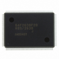
HD64F2638F20J Renesas Electronics America, HD64F2638F20J Datasheet - Page 596

HD64F2638F20J
Manufacturer Part Number
HD64F2638F20J
Description
IC H8S MCU FLASH 256K 128-QFP
Manufacturer
Renesas Electronics America
Series
H8® H8S/2600r
Specifications of HD64F2638F20J
Core Processor
H8S/2600
Core Size
16-Bit
Speed
20MHz
Connectivity
CAN, SCI, SmartCard
Peripherals
Motor Control PWM, POR, PWM, WDT
Number Of I /o
72
Program Memory Size
256KB (256K x 8)
Program Memory Type
FLASH
Ram Size
16K x 8
Voltage - Supply (vcc/vdd)
4.5 V ~ 5.5 V
Data Converters
A/D 12x10b; D/A 2x8b
Oscillator Type
Internal
Operating Temperature
-40°C ~ 85°C
Package / Case
128-QFP
Lead Free Status / RoHS Status
Contains lead / RoHS non-compliant
Eeprom Size
-
Available stocks
Company
Part Number
Manufacturer
Quantity
Price
Company:
Part Number:
HD64F2638F20J
Manufacturer:
PENESAS
Quantity:
252
- Current page: 596 of 1512
- Download datasheet (9Mb)
Section 15 I
(Only for the H8S/2638, H8S/2639, and H8S/2630)
• Wait function in slave mode (I
• Three interrupt sources
• Selection of 16 internal clocks (in master mode)
• Direct bus drive (with SCL and SDA pins)
15.1.2
Figure 15-1 shows a block diagram of the I
Figure 15-2 shows an example of I/O pin connections to external circuits. Channel 0 I/O pins are
NMOS open drains, and it is possible to apply voltages in excess of the power supply (V
voltage for this LSI. Set the upper limit of voltage applied to the power supply (V
range + 0.3 V, i.e. 5.8 V. Channel 1 I/O pins are driven solely by NMOS, so in terms of
appearance they carry out the same operations as an NMOS open drain. However, the voltage
which can be applied to the I/O pins depends on the voltage of the power supply (V
Page 546 of 1458
⎯ A wait request can be generated by driving the SCL pin low after data transfer, excluding
⎯ Data transfer end (including transmission mode transition with I
⎯ Address match: when any slave address matches or the general call address is received in
⎯ Stop condition detection
⎯ Two pins—P35/SCL0 and P34/SDA0—(normally NMOS push-pull outputs) function as
⎯ Two pins—P33/SCL1 and P32/SDA1—(normally CMOS pins) function as NMOS-only
acknowledgement. The wait request is cleared when the next transfer becomes possible.
reception after loss of master arbitration)
slave receive mode (I
NMOS open-drain outputs when the bus drive function is selected.
outputs when the bus drive function is selected.
Block Diagram
2
C Bus Interface [Option]
2
C bus format)
2
C bus format)
2
C bus interface.
2
C bus format and address
H8S/2639, H8S/2638, H8S/2636,
REJ09B0103-0800 Rev. 8.00
H8S/2630, H8S/2635 Group
CC
CC
) power supply
) of this LSI.
May 28, 2010
CC
)
Related parts for HD64F2638F20J
Image
Part Number
Description
Manufacturer
Datasheet
Request
R

Part Number:
Description:
KIT STARTER FOR M16C/29
Manufacturer:
Renesas Electronics America
Datasheet:

Part Number:
Description:
KIT STARTER FOR R8C/2D
Manufacturer:
Renesas Electronics America
Datasheet:

Part Number:
Description:
R0K33062P STARTER KIT
Manufacturer:
Renesas Electronics America
Datasheet:

Part Number:
Description:
KIT STARTER FOR R8C/23 E8A
Manufacturer:
Renesas Electronics America
Datasheet:

Part Number:
Description:
KIT STARTER FOR R8C/25
Manufacturer:
Renesas Electronics America
Datasheet:

Part Number:
Description:
KIT STARTER H8S2456 SHARPE DSPLY
Manufacturer:
Renesas Electronics America
Datasheet:

Part Number:
Description:
KIT STARTER FOR R8C38C
Manufacturer:
Renesas Electronics America
Datasheet:

Part Number:
Description:
KIT STARTER FOR R8C35C
Manufacturer:
Renesas Electronics America
Datasheet:

Part Number:
Description:
KIT STARTER FOR R8CL3AC+LCD APPS
Manufacturer:
Renesas Electronics America
Datasheet:

Part Number:
Description:
KIT STARTER FOR RX610
Manufacturer:
Renesas Electronics America
Datasheet:

Part Number:
Description:
KIT STARTER FOR R32C/118
Manufacturer:
Renesas Electronics America
Datasheet:

Part Number:
Description:
KIT DEV RSK-R8C/26-29
Manufacturer:
Renesas Electronics America
Datasheet:

Part Number:
Description:
KIT STARTER FOR SH7124
Manufacturer:
Renesas Electronics America
Datasheet:

Part Number:
Description:
KIT STARTER FOR H8SX/1622
Manufacturer:
Renesas Electronics America
Datasheet:


