MC68302EH16C Freescale Semiconductor, MC68302EH16C Datasheet - Page 143
MC68302EH16C
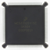
Manufacturer Part Number
MC68302EH16C
Description
IC MPU MULTI-PROTOCOL 132-PQFP
Manufacturer
Freescale Semiconductor
Datasheets
1.MC68302AG20C.pdf
(4 pages)
2.MC68302AG20C.pdf
(2 pages)
3.MC68302AG20C.pdf
(13 pages)
4.MC68302EH16C.pdf
(481 pages)
Specifications of MC68302EH16C
Processor Type
M683xx 32-Bit
Speed
16MHz
Voltage
5V
Mounting Type
Surface Mount
Package / Case
132-MQFP, 132-PQFP
Controller Family/series
68K
Core Size
32 Bit
Ram Memory Size
1152Byte
Cpu Speed
16MHz
No. Of Timers
3
Embedded Interface Type
SCP, TDM
Digital Ic Case Style
PQFP
Rohs Compliant
Yes
Family Name
M68000
Device Core
ColdFire
Device Core Size
32b
Frequency (max)
16MHz
Instruction Set Architecture
RISC
Supply Voltage 1 (typ)
5V
Operating Temp Range
0C to 70C
Operating Temperature Classification
Commercial
Mounting
Surface Mount
Pin Count
132
Package Type
PQFP
Lead Free Status / RoHS Status
Lead free / RoHS Compliant
Features
-
Lead Free Status / Rohs Status
RoHS Compliant part
Electrostatic Device
Available stocks
Company
Part Number
Manufacturer
Quantity
Price
Company:

Part Number:
MC68302EH16C
Manufacturer:
Freescale Semiconductor
Quantity:
135
Company:
Part Number:
MC68302EH16C
Manufacturer:
PANA
Quantity:
99
Company:
Part Number:
MC68302EH16C
Manufacturer:
Freescale Semiconductor
Quantity:
10 000
Part Number:
MC68302EH16C
Manufacturer:
FREESCALE
Quantity:
20 000
Company:
Part Number:
MC68302EH16CB1
Manufacturer:
Freescale Semiconductor
Quantity:
10 000
Company:
Part Number:
MC68302EH16CR2
Manufacturer:
Freescale Semiconductor
Quantity:
10 000


Communications Processor (CP)
three channels of a PCM highway. Each protocol-type implementation uses identical buffer
structures to simplify programming.
The following protocols are supported: HDLC/SDLC, BISYNC, synchronous and asynchro-
nous DDCMP, UART, several transparent modes, and V.110 rate adaption support. Each
protocol can be implemented with IDL, GCI, PCM, or NMSI physical layer interfaces (see
4.4 Serial Channels Physical Interface) and can be configured to operate in either echo or
loopback mode. Echo mode provides a return signal from an SCC by retransmitting the re-
ceived signal. Loopback mode is a local feedback connection allowing an SCC to receive
the signal it is transmitting. (Echo and loopback mode for multiplexed interfaces are dis-
cussed in 4.4 Serial Channels Physical Interface).
The receive and transmit section of each SCC is supported with one of the six dedicated
SDMA channels (see 4.2 SDMA Channels). These channels transfer data between the
SCCs and either external RAM or on-chip dual-port RAM. This function is transparent to the
user, being enabled and controlled according to the configuration of each SCC channel.
Each SCC can be clocked by either an external source (with the clock pins RCLK or TCLK)
or by an internal source through a baud rate generator for each SCC channel. The baud rate
generator can derive its clock from the main IMP clock or from a separate input clock. The
SCC transmitter and receiver sections are independent and may be clocked at different
rates.
The SCCs exhibit two types of performance limitations. The first type is a hardware clocking
limit, which is the same for each SCC. The SCC clocks must not exceed a ratio of 1:2.5 serial
clock (RCLK or TCLK) to parallel clock (EXTAL). Thus, for a 16.67-MHz system clock fre-
quency, the serial clock must not exceed 6.67 MHz. The second type concerns the system
data rate. The SDMA channels and CP main controller must have enough time to service
the SCCs, thus preventing FIFO underruns and overruns in the SCCs. This requirement de-
pends on a number of factors discussed in more detail in Appendix A SCC Performance.
Each SCC supports the standard seven-line modem interface (also referred to as NMSI)
with the signals RXD, TXD, RCLK, TCLK, RTS, CTS, and CD. Other modem signals (such
as DSR and DTR) may be supported through the parallel I/O pins. A block diagram of the
SCC is depicted in Figure 4-11.
To provide extra modem serial output lines, the user must define I/O port A or B pins as out-
puts in the port A/B data direction register and write to the port A/B data register to cause
the state of the pin to change. Extra serial input lines with interrupts may be supported by
defining the port B pins as inputs in the port B data direction register. When a change in the
state of the pin occurs, the interrupt handler may assert or negate the extra outputs to sup-
port the hand-shaking protocol. (See 3.3 Parallel I/O Ports for related details.)
MOTOROLA
MC68302 USER’S MANUAL
4-23
Related parts for MC68302EH16C
Image
Part Number
Description
Manufacturer
Datasheet
Request
R

Part Number:
Description:
Manufacturer:
Freescale Semiconductor, Inc
Datasheet:

Part Number:
Description:
MC68302 Configuring the Chip Selects on the MC68302
Manufacturer:
Motorola / Freescale Semiconductor
Part Number:
Description:
MC68302 Design Concept - Expanding Interrupts on the MC68302
Manufacturer:
Motorola / Freescale Semiconductor
Part Number:
Description:
MC68302 MC68302 Adapting a WAN Controller to a LAN Environment
Manufacturer:
Motorola / Freescale Semiconductor
Part Number:
Description:
MC68302 EKB Applications - Power Measurements on the MC68302
Manufacturer:
Motorola / Freescale Semiconductor
Part Number:
Description:
MC68302 Interfacing the MC68020 to a Slave MC68302
Manufacturer:
Motorola / Freescale Semiconductor
Part Number:
Description:
MC68302 MC68302 Software Performance
Manufacturer:
Motorola / Freescale Semiconductor
Part Number:
Description:
MC68302 Evaluating EDX on the ADS302
Manufacturer:
Motorola / Freescale Semiconductor
Part Number:
Description:
MC68302 Design Advisory #1 - MC68SC302 Passive ISDN Protocol Engine
Manufacturer:
Motorola / Freescale Semiconductor
Part Number:
Description:
MC68302, MC68360, and MPC860 Characteristics and Design Notes for Crystal Feedback Oscillators
Manufacturer:
Motorola / Freescale Semiconductor
Part Number:
Description:
Mc68302 Integrated Multi-protocol Processor
Manufacturer:
Freescale Semiconductor, Inc
Datasheet:
Part Number:
Description:
Manufacturer:
Freescale Semiconductor, Inc
Datasheet:
Part Number:
Description:
Manufacturer:
Freescale Semiconductor, Inc
Datasheet:
Part Number:
Description:
Manufacturer:
Freescale Semiconductor, Inc
Datasheet:
Part Number:
Description:
Manufacturer:
Freescale Semiconductor, Inc
Datasheet: