MC68302EH16C Freescale Semiconductor, MC68302EH16C Datasheet - Page 273
MC68302EH16C
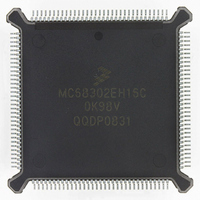
Manufacturer Part Number
MC68302EH16C
Description
IC MPU MULTI-PROTOCOL 132-PQFP
Manufacturer
Freescale Semiconductor
Datasheets
1.MC68302AG20C.pdf
(4 pages)
2.MC68302AG20C.pdf
(2 pages)
3.MC68302AG20C.pdf
(13 pages)
4.MC68302EH16C.pdf
(481 pages)
Specifications of MC68302EH16C
Processor Type
M683xx 32-Bit
Speed
16MHz
Voltage
5V
Mounting Type
Surface Mount
Package / Case
132-MQFP, 132-PQFP
Controller Family/series
68K
Core Size
32 Bit
Ram Memory Size
1152Byte
Cpu Speed
16MHz
No. Of Timers
3
Embedded Interface Type
SCP, TDM
Digital Ic Case Style
PQFP
Rohs Compliant
Yes
Family Name
M68000
Device Core
ColdFire
Device Core Size
32b
Frequency (max)
16MHz
Instruction Set Architecture
RISC
Supply Voltage 1 (typ)
5V
Operating Temp Range
0C to 70C
Operating Temperature Classification
Commercial
Mounting
Surface Mount
Pin Count
132
Package Type
PQFP
Lead Free Status / RoHS Status
Lead free / RoHS Compliant
Features
-
Lead Free Status / Rohs Status
RoHS Compliant part
Electrostatic Device
Available stocks
Company
Part Number
Manufacturer
Quantity
Price
Company:

Part Number:
MC68302EH16C
Manufacturer:
Freescale Semiconductor
Quantity:
135
Company:
Part Number:
MC68302EH16C
Manufacturer:
PANA
Quantity:
99
Company:
Part Number:
MC68302EH16C
Manufacturer:
Freescale Semiconductor
Quantity:
10 000
Part Number:
MC68302EH16C
Manufacturer:
FREESCALE
Quantity:
20 000
Company:
Part Number:
MC68302EH16CB1
Manufacturer:
Freescale Semiconductor
Quantity:
10 000
Company:
Part Number:
MC68302EH16CR2
Manufacturer:
Freescale Semiconductor
Quantity:
10 000


RMC/IOUT1—Read-Modify-Write Cycle Indication/Interrupt Output 1
IAC—Internal Access
MOTOROLA
ters. If DTACK is generated internally, then it is an output. It is an input when the IMP ac-
cesses an external device not within the range of the chip-select logic or when
programmed to be generated externally.
This signal functions as RMC in normal operation. RMC is an output signal that is asserted
when a read-modify-write cycle is executed. It indicates that the cycle is indivisible.
When the M68000 core is disabled, this pin operates as IOUT1. IOUT2–IOUT0 provide
the interrupt request output signals from the IMP interrupt controller to an external CPU
when the M68000 core is disabled.
This output indicates that the current bus cycle accesses an on-chip location. This in-
cludes the on-chip 4K byte block of internal RAM and registers (both real and reserved
locations), and the system configuration registers ($0F0–$0FF). The above-mentioned
bus cycle may originate from the M68000 core, the IDMA, or an external bus master. Note
that, if the SDMA accesses the internal dual-port RAM, it does so without arbitration on
the M68000 bus; therefore, the IAC pin is not asserted in this case. The timing of IAC is
identical to that of the CS3–CS0 pins.
IAC can be used to disable an external address/data buffer when the on-chip dual-port
RAM and registers are accessed, thus preventing bus contention. Such a buffer is option-
al and is only required in larger systems. An external address/data buffer with its output
enable (E) and direction control (dir) may be placed between the two bus segments as
shown in Figure 5-7. The IAC signal saves the propagation delay and logic required to OR
all the various system chip-select lines together to determine when to enable the external
buffers.
RAM
IMP
IAC
Figure 5-7. External Address/Data Buffer
E
MC68302 USER’S MANUAL
OTHER MASTER/SLAVE
BUFFERS
ROM
DIR
OTHER MASTER/SLAVE
OTHER SLAVE
R/W
Signal Description
5-9
Related parts for MC68302EH16C
Image
Part Number
Description
Manufacturer
Datasheet
Request
R

Part Number:
Description:
Manufacturer:
Freescale Semiconductor, Inc
Datasheet:

Part Number:
Description:
MC68302 Configuring the Chip Selects on the MC68302
Manufacturer:
Motorola / Freescale Semiconductor
Part Number:
Description:
MC68302 Design Concept - Expanding Interrupts on the MC68302
Manufacturer:
Motorola / Freescale Semiconductor
Part Number:
Description:
MC68302 MC68302 Adapting a WAN Controller to a LAN Environment
Manufacturer:
Motorola / Freescale Semiconductor
Part Number:
Description:
MC68302 EKB Applications - Power Measurements on the MC68302
Manufacturer:
Motorola / Freescale Semiconductor
Part Number:
Description:
MC68302 Interfacing the MC68020 to a Slave MC68302
Manufacturer:
Motorola / Freescale Semiconductor
Part Number:
Description:
MC68302 MC68302 Software Performance
Manufacturer:
Motorola / Freescale Semiconductor
Part Number:
Description:
MC68302 Evaluating EDX on the ADS302
Manufacturer:
Motorola / Freescale Semiconductor
Part Number:
Description:
MC68302 Design Advisory #1 - MC68SC302 Passive ISDN Protocol Engine
Manufacturer:
Motorola / Freescale Semiconductor
Part Number:
Description:
MC68302, MC68360, and MPC860 Characteristics and Design Notes for Crystal Feedback Oscillators
Manufacturer:
Motorola / Freescale Semiconductor
Part Number:
Description:
Mc68302 Integrated Multi-protocol Processor
Manufacturer:
Freescale Semiconductor, Inc
Datasheet:
Part Number:
Description:
Manufacturer:
Freescale Semiconductor, Inc
Datasheet:
Part Number:
Description:
Manufacturer:
Freescale Semiconductor, Inc
Datasheet:
Part Number:
Description:
Manufacturer:
Freescale Semiconductor, Inc
Datasheet:
Part Number:
Description:
Manufacturer:
Freescale Semiconductor, Inc
Datasheet: