MC68302EH16C Freescale Semiconductor, MC68302EH16C Datasheet - Page 393
MC68302EH16C
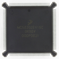
Manufacturer Part Number
MC68302EH16C
Description
IC MPU MULTI-PROTOCOL 132-PQFP
Manufacturer
Freescale Semiconductor
Datasheets
1.MC68302AG20C.pdf
(4 pages)
2.MC68302AG20C.pdf
(2 pages)
3.MC68302AG20C.pdf
(13 pages)
4.MC68302EH16C.pdf
(481 pages)
Specifications of MC68302EH16C
Processor Type
M683xx 32-Bit
Speed
16MHz
Voltage
5V
Mounting Type
Surface Mount
Package / Case
132-MQFP, 132-PQFP
Controller Family/series
68K
Core Size
32 Bit
Ram Memory Size
1152Byte
Cpu Speed
16MHz
No. Of Timers
3
Embedded Interface Type
SCP, TDM
Digital Ic Case Style
PQFP
Rohs Compliant
Yes
Family Name
M68000
Device Core
ColdFire
Device Core Size
32b
Frequency (max)
16MHz
Instruction Set Architecture
RISC
Supply Voltage 1 (typ)
5V
Operating Temp Range
0C to 70C
Operating Temperature Classification
Commercial
Mounting
Surface Mount
Pin Count
132
Package Type
PQFP
Lead Free Status / RoHS Status
Lead free / RoHS Compliant
Features
-
Lead Free Status / Rohs Status
RoHS Compliant part
Electrostatic Device
Available stocks
Company
Part Number
Manufacturer
Quantity
Price
Company:

Part Number:
MC68302EH16C
Manufacturer:
Freescale Semiconductor
Quantity:
135
Company:
Part Number:
MC68302EH16C
Manufacturer:
PANA
Quantity:
99
Company:
Part Number:
MC68302EH16C
Manufacturer:
Freescale Semiconductor
Quantity:
10 000
Part Number:
MC68302EH16C
Manufacturer:
FREESCALE
Quantity:
20 000
Company:
Part Number:
MC68302EH16CB1
Manufacturer:
Freescale Semiconductor
Quantity:
10 000
Company:
Part Number:
MC68302EH16CR2
Manufacturer:
Freescale Semiconductor
Quantity:
10 000


MC68302 Applications
for a given protocol. For HDLC and transparent, this is every 16 bits; whereas, in the other
protocols, it is every 8 bits on receive and every 16 bits on transmit.
This application does not address the issue of choosing whether a master-slave arrange-
ment is the best approach for your application, but rather looks at the design issues that
need to be addressed once the approach seems reasonable. (Most applications usually find
the master-slave approach shown in Figure D-19 quite acceptable for data rates up to 64
kbps on each of the nine SCCs. Any comments on rates beyond this value tend to be less
general and more application dependent.)
D.7.1 Synchronous vs. Asynchronous Accesses
When a device is in slave mode, there are two different ways it can be accessed: synchro-
nously and asynchronously.
When the MC68302 enters slave mode, it is initialized with asynchronous accesses. The
term “asynchronous” refers to the fact that the master does not need to supply signals to the
slave on particular system clock edges, as required in synchronous. However, asynchro-
nous accesses are always and only three waits states for both reads and writes. In general,
this is the suggested method of accessing the MC68302 in slave mode. These accesses are
much simpler than in synchronous timing. Any performance loss is minimal since, once the
MC68302 is initialized, accesses to it are rare. The SDMA channels, which are unaffected
by this choice, can still operate with zero wait states and comprise most of the slave
MC68302 activity.
If the SAM bit in the SCR is set, the following accesses to the slave MC68302 will be syn-
chronous. Writes will be zero wait states, and reads can be either zero or one wait state,
based on the EMWS bit in the SCR. The EMWS bit is almost always required to meet syn-
chronous setup times. Synchronous accesses should be used when one master MC68302
is accessing another slave MC68302 without any intervening glue (like buffers). In this case,
the synchronous timings can be met with proper clocking.
D.7.2 Clocking
The master clock out (CLKO) line should be connected to the EXTAL input of the slaves,
allowing the master MC68302 to perform zero wait state writes and one wait state reads
from the slave MC68302 at full 16.67-MHz operation in synchronous mode. The guaranteed
propagation delay between EXTAL and CLKO is 2-11 ns at 16.67-MHz operation. The typ-
ical delay is about 5 ns.
If a single external clock is required to drive the inputs to all the MC68302 EXTAL pins, the
skew between EXTAL and CLKO must be watched by the designer. In the case of synchro-
nous accesses, this will certainly slow the overall frequency that can be designed.
D.7.3 Programming the Base Address Registers (BARs)
The next issue is how to program the three BARs on each of the MC68302s considering they
have the same address ($0F2). Figure D-19 shows an easy method of programming the
BAR. The master MC68302 first programs its BAR at $0000F2. For each slave, it writes the
slave's parallel l/O line with a zero and writes to $8000F2 to program the slave's BAR. This
MOTOROLA
MC68302 USER’S MANUAL
D-43
Related parts for MC68302EH16C
Image
Part Number
Description
Manufacturer
Datasheet
Request
R

Part Number:
Description:
Manufacturer:
Freescale Semiconductor, Inc
Datasheet:

Part Number:
Description:
MC68302 Configuring the Chip Selects on the MC68302
Manufacturer:
Motorola / Freescale Semiconductor
Part Number:
Description:
MC68302 Design Concept - Expanding Interrupts on the MC68302
Manufacturer:
Motorola / Freescale Semiconductor
Part Number:
Description:
MC68302 MC68302 Adapting a WAN Controller to a LAN Environment
Manufacturer:
Motorola / Freescale Semiconductor
Part Number:
Description:
MC68302 EKB Applications - Power Measurements on the MC68302
Manufacturer:
Motorola / Freescale Semiconductor
Part Number:
Description:
MC68302 Interfacing the MC68020 to a Slave MC68302
Manufacturer:
Motorola / Freescale Semiconductor
Part Number:
Description:
MC68302 MC68302 Software Performance
Manufacturer:
Motorola / Freescale Semiconductor
Part Number:
Description:
MC68302 Evaluating EDX on the ADS302
Manufacturer:
Motorola / Freescale Semiconductor
Part Number:
Description:
MC68302 Design Advisory #1 - MC68SC302 Passive ISDN Protocol Engine
Manufacturer:
Motorola / Freescale Semiconductor
Part Number:
Description:
MC68302, MC68360, and MPC860 Characteristics and Design Notes for Crystal Feedback Oscillators
Manufacturer:
Motorola / Freescale Semiconductor
Part Number:
Description:
Mc68302 Integrated Multi-protocol Processor
Manufacturer:
Freescale Semiconductor, Inc
Datasheet:
Part Number:
Description:
Manufacturer:
Freescale Semiconductor, Inc
Datasheet:
Part Number:
Description:
Manufacturer:
Freescale Semiconductor, Inc
Datasheet:
Part Number:
Description:
Manufacturer:
Freescale Semiconductor, Inc
Datasheet:
Part Number:
Description:
Manufacturer:
Freescale Semiconductor, Inc
Datasheet: