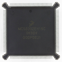
MC68302EH16C Freescale Semiconductor, MC68302EH16C Datasheet - Page 229

MC68302EH16C
Manufacturer Part Number
MC68302EH16C
Description
IC MPU MULTI-PROTOCOL 132-PQFP
Manufacturer
Freescale Semiconductor
Datasheets
1.MC68302AG20C.pdf
(4 pages)
2.MC68302AG20C.pdf
(2 pages)
3.MC68302AG20C.pdf
(13 pages)
4.MC68302EH16C.pdf
(481 pages)
Specifications of MC68302EH16C
Processor Type
M683xx 32-Bit
Speed
16MHz
Voltage
5V
Mounting Type
Surface Mount
Package / Case
132-MQFP, 132-PQFP
Controller Family/series
68K
Core Size
32 Bit
Ram Memory Size
1152Byte
Cpu Speed
16MHz
No. Of Timers
3
Embedded Interface Type
SCP, TDM
Digital Ic Case Style
PQFP
Rohs Compliant
Yes
Family Name
M68000
Device Core
ColdFire
Device Core Size
32b
Frequency (max)
16MHz
Instruction Set Architecture
RISC
Supply Voltage 1 (typ)
5V
Operating Temp Range
0C to 70C
Operating Temperature Classification
Commercial
Mounting
Surface Mount
Pin Count
132
Package Type
PQFP
Lead Free Status / RoHS Status
Lead free / RoHS Compliant
Features
-
Lead Free Status / Rohs Status
RoHS Compliant part
Electrostatic Device
Available stocks
Company
Part Number
Manufacturer
Quantity
Price
Company:
Part Number:
MC68302EH16C
Manufacturer:
Freescale Semiconductor
Quantity:
135
Company:
Part Number:
MC68302EH16C
Manufacturer:
PANA
Quantity:
99
Company:
Part Number:
MC68302EH16C
Manufacturer:
Freescale Semiconductor
Quantity:
10 000
Part Number:
MC68302EH16C
Manufacturer:
FREESCALE
Quantity:
20 000
Company:
Part Number:
MC68302EH16CB1
Manufacturer:
Freescale Semiconductor
Quantity:
10 000
Company:
Part Number:
MC68302EH16CR2
Manufacturer:
Freescale Semiconductor
Quantity:
10 000
- MC68302AG20C PDF datasheet
- MC68302AG20C PDF datasheet #2
- MC68302AG20C PDF datasheet #3
- MC68302EH16C PDF datasheet #4
- Current page: 229 of 481
- Download datasheet (2Mb)
OFFSET + 0
OFFSET + 2
OFFSET + 4
Bits 11, 9–8—Reserved for future use.
V.110—V.110 Mode
SYNF—Transmit SYN1–SYN2 or IDLE between Messages and Control the RTS Pin
The DDCMP controller can transmit ones in both NRZ and NRZI data encoded formats. The
minimum number of ones transmitted is 17.
ENC—Data Encoding Format
COMMON SCC MODE BITS—See 4.5.3 SCC Mode Register (SCM) for a description of the
DIAG1, DIAG0, ENR, ENT, MODE1, and MODE0 bits.
4.5.14.10 DDCMP Receive Buffer Descriptor (Rx BD)
The CP reports information about the received data for each buffer using the BDs. The Rx
BD is shown in Figure 4-36. The CP closes the current buffer, generates a maskable inter-
rupt, and starts to receive data in the next buffer after any of the following events:
OFFSET +6
The first word of the Rx BD contains control and status bits. Bits 15–12 are written by the
user before the buffer is linked to the Rx BD table, and bits 5–0 and 11–8 are set by the IMP
MOTOROLA
• Receiving the received message length number of bytes (RMLG)
• Detecting an error
• Detecting a full receive buffer
• Issuing the ENTER HUNT MODE command
0 = DDCMP mode; synchronous DDCMP is chosen.
1 = V.110 mode; the V.110 protocol description is in 4.5.15 V.110 Controller.
0 = Send ones between messages. RTS is negated between messages.
1 = Send SYN1–SYN2 pairs between messages. RTS is always asserted. Note that
0 = Nonreturn to Zero (NRZ). A one is a high level; a zero is a low level.
1 = Nonreturn to Zero Inverted (NRZI). A one is represented by no change in the level;
SYN1 and SYN2 may be the same character.
a zero is represented by a change in the level. The receiver decodes NRZI, but a
clock must be supplied. The transmitter encodes NRZI.
15
E
14
X
Figure 4-36. DDCMP Receive Buffer Descriptor
13
W
12
I
RX BUFFER POINTER (24-bits used, upper 8 bits must be 0)
11
L
MC68302 USER’S MANUAL
10
H
T2
9
NOTE
DATA LENGTH
T1
8
—
7
—
6
Communications Processor (CP)
CF
5
FR
4
PR
3
CR
2
OV
1
4-109
CD
0
Related parts for MC68302EH16C
Image
Part Number
Description
Manufacturer
Datasheet
Request
R
Part Number:
Description:
Manufacturer:
Freescale Semiconductor, Inc
Datasheet:

Part Number:
Description:
MC68302 Configuring the Chip Selects on the MC68302
Manufacturer:
Motorola / Freescale Semiconductor

Part Number:
Description:
MC68302 Design Concept - Expanding Interrupts on the MC68302
Manufacturer:
Motorola / Freescale Semiconductor

Part Number:
Description:
MC68302 MC68302 Adapting a WAN Controller to a LAN Environment
Manufacturer:
Motorola / Freescale Semiconductor

Part Number:
Description:
MC68302 EKB Applications - Power Measurements on the MC68302
Manufacturer:
Motorola / Freescale Semiconductor

Part Number:
Description:
MC68302 Interfacing the MC68020 to a Slave MC68302
Manufacturer:
Motorola / Freescale Semiconductor

Part Number:
Description:
MC68302 MC68302 Software Performance
Manufacturer:
Motorola / Freescale Semiconductor

Part Number:
Description:
MC68302 Evaluating EDX on the ADS302
Manufacturer:
Motorola / Freescale Semiconductor

Part Number:
Description:
MC68302 Design Advisory #1 - MC68SC302 Passive ISDN Protocol Engine
Manufacturer:
Motorola / Freescale Semiconductor

Part Number:
Description:
MC68302, MC68360, and MPC860 Characteristics and Design Notes for Crystal Feedback Oscillators
Manufacturer:
Motorola / Freescale Semiconductor
Part Number:
Description:
Mc68302 Integrated Multi-protocol Processor
Manufacturer:
Freescale Semiconductor, Inc
Datasheet:
Part Number:
Description:
Manufacturer:
Freescale Semiconductor, Inc
Datasheet:
Part Number:
Description:
Manufacturer:
Freescale Semiconductor, Inc
Datasheet:
Part Number:
Description:
Manufacturer:
Freescale Semiconductor, Inc
Datasheet:
Part Number:
Description:
Manufacturer:
Freescale Semiconductor, Inc
Datasheet:


