MC68302EH16C Freescale Semiconductor, MC68302EH16C Datasheet - Page 145
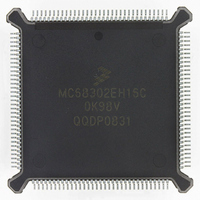
MC68302EH16C
Manufacturer Part Number
MC68302EH16C
Description
IC MPU MULTI-PROTOCOL 132-PQFP
Manufacturer
Freescale Semiconductor
Datasheets
1.MC68302AG20C.pdf
(4 pages)
2.MC68302AG20C.pdf
(2 pages)
3.MC68302AG20C.pdf
(13 pages)
4.MC68302EH16C.pdf
(481 pages)
Specifications of MC68302EH16C
Processor Type
M683xx 32-Bit
Speed
16MHz
Voltage
5V
Mounting Type
Surface Mount
Package / Case
132-MQFP, 132-PQFP
Controller Family/series
68K
Core Size
32 Bit
Ram Memory Size
1152Byte
Cpu Speed
16MHz
No. Of Timers
3
Embedded Interface Type
SCP, TDM
Digital Ic Case Style
PQFP
Rohs Compliant
Yes
Family Name
M68000
Device Core
ColdFire
Device Core Size
32b
Frequency (max)
16MHz
Instruction Set Architecture
RISC
Supply Voltage 1 (typ)
5V
Operating Temp Range
0C to 70C
Operating Temperature Classification
Commercial
Mounting
Surface Mount
Pin Count
132
Package Type
PQFP
Lead Free Status / RoHS Status
Lead free / RoHS Compliant
Features
-
Lead Free Status / Rohs Status
RoHS Compliant part
Electrostatic Device
Available stocks
Company
Part Number
Manufacturer
Quantity
Price
Company:

Part Number:
MC68302EH16C
Manufacturer:
Freescale Semiconductor
Quantity:
135
Company:
Part Number:
MC68302EH16C
Manufacturer:
PANA
Quantity:
99
Company:
Part Number:
MC68302EH16C
Manufacturer:
Freescale Semiconductor
Quantity:
10 000
Part Number:
MC68302EH16C
Manufacturer:
FREESCALE
Quantity:
20 000
Company:
Part Number:
MC68302EH16CB1
Manufacturer:
Freescale Semiconductor
Quantity:
10 000
Company:
Part Number:
MC68302EH16CR2
Manufacturer:
Freescale Semiconductor
Quantity:
10 000


Each SCON is a 16-bit, memory-mapped, read-write register. The SCONs are set to $0004
by reset, resulting in the baud rate generator output clock rate being set to the main clock
rate divided by 3. The baud rate generator output clock is always available externally, as
shown in Table 5-8.
WOMS—Wired-OR
EXTC—External Clock
TCS—Transmit Clock Source
RCS—Receive Clock Source
MOTOROLA
WOMS
When WOMS is set, the TXD driver is programmed to function as an open-drain output
and may be externally wired together with other TXD pins in an appropriate bus configu-
ration. In this case, an external pullup resistor is required. When WOMS is cleared, the
TXD pin operates normally with an active internal pullup.
The EXTC bit selects whether the baud rate generator input clock source is the internal
main clock (EXTC = 0) or external clock (EXTC = 1). If EXTC = 1, the external clock is
taken from the TIN1 pin. Note that the single TIN1 pin can be used to supply a clock for
all three baud rate generators.
The TCS bit selects either the baud rate generator output (TCS = 0) or the TCLK pin (TCS
= 1) for the transmitter clock. If TCS = 0, then the baud rate generator output is driven onto
the TCLK pin. This bit should be programmed to one if a multiplexed mode is chosen for
the SCC.
After system reset, SCC hardware causes TCLK to default to an input and stay an input
until a zero is written to TCS. For SCC2 and SCC3, TCLK can be derived directly from the
RCLK pin as shown in Table 3-6.
The RCS bit selects either the baud rate generator output (RCS = 0) or the RCLK pin
(RCS = 1) for the receiver clock. If RCS = 0, then the baud rate generator output is driven
onto the RCLK pin. This bit should be programmed to one if a multiplexed mode is chosen
for the SCC.
After system reset, SCC hardware causes the RCLK to default to an input and stay an
input until a zero is written to RCS.
15
EXTC
14
TCS
The BRG output are 180 degrees out of phase to the TCLK and
RCLK signals used by the SCC and output on the RCLK and
TCLK pins.
13
RCS
12
CD10
11
This bit is valid only in NMSI mode.
CD9
10
MC68302 USER’S MANUAL
CD8
9
CD7
NOTE
NOTE
8
CD6
7
CD5
6
CD4
5
Communications Processor (CP)
CD3
4
CD2
3
CD1
2
CD0
1
DIV4
4-25
0
Related parts for MC68302EH16C
Image
Part Number
Description
Manufacturer
Datasheet
Request
R

Part Number:
Description:
Manufacturer:
Freescale Semiconductor, Inc
Datasheet:

Part Number:
Description:
MC68302 Configuring the Chip Selects on the MC68302
Manufacturer:
Motorola / Freescale Semiconductor
Part Number:
Description:
MC68302 Design Concept - Expanding Interrupts on the MC68302
Manufacturer:
Motorola / Freescale Semiconductor
Part Number:
Description:
MC68302 MC68302 Adapting a WAN Controller to a LAN Environment
Manufacturer:
Motorola / Freescale Semiconductor
Part Number:
Description:
MC68302 EKB Applications - Power Measurements on the MC68302
Manufacturer:
Motorola / Freescale Semiconductor
Part Number:
Description:
MC68302 Interfacing the MC68020 to a Slave MC68302
Manufacturer:
Motorola / Freescale Semiconductor
Part Number:
Description:
MC68302 MC68302 Software Performance
Manufacturer:
Motorola / Freescale Semiconductor
Part Number:
Description:
MC68302 Evaluating EDX on the ADS302
Manufacturer:
Motorola / Freescale Semiconductor
Part Number:
Description:
MC68302 Design Advisory #1 - MC68SC302 Passive ISDN Protocol Engine
Manufacturer:
Motorola / Freescale Semiconductor
Part Number:
Description:
MC68302, MC68360, and MPC860 Characteristics and Design Notes for Crystal Feedback Oscillators
Manufacturer:
Motorola / Freescale Semiconductor
Part Number:
Description:
Mc68302 Integrated Multi-protocol Processor
Manufacturer:
Freescale Semiconductor, Inc
Datasheet:
Part Number:
Description:
Manufacturer:
Freescale Semiconductor, Inc
Datasheet:
Part Number:
Description:
Manufacturer:
Freescale Semiconductor, Inc
Datasheet:
Part Number:
Description:
Manufacturer:
Freescale Semiconductor, Inc
Datasheet:
Part Number:
Description:
Manufacturer:
Freescale Semiconductor, Inc
Datasheet: