MC68302EH16C Freescale Semiconductor, MC68302EH16C Datasheet - Page 387
MC68302EH16C
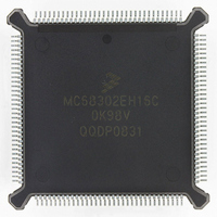
Manufacturer Part Number
MC68302EH16C
Description
IC MPU MULTI-PROTOCOL 132-PQFP
Manufacturer
Freescale Semiconductor
Datasheets
1.MC68302AG20C.pdf
(4 pages)
2.MC68302AG20C.pdf
(2 pages)
3.MC68302AG20C.pdf
(13 pages)
4.MC68302EH16C.pdf
(481 pages)
Specifications of MC68302EH16C
Processor Type
M683xx 32-Bit
Speed
16MHz
Voltage
5V
Mounting Type
Surface Mount
Package / Case
132-MQFP, 132-PQFP
Controller Family/series
68K
Core Size
32 Bit
Ram Memory Size
1152Byte
Cpu Speed
16MHz
No. Of Timers
3
Embedded Interface Type
SCP, TDM
Digital Ic Case Style
PQFP
Rohs Compliant
Yes
Family Name
M68000
Device Core
ColdFire
Device Core Size
32b
Frequency (max)
16MHz
Instruction Set Architecture
RISC
Supply Voltage 1 (typ)
5V
Operating Temp Range
0C to 70C
Operating Temperature Classification
Commercial
Mounting
Surface Mount
Pin Count
132
Package Type
PQFP
Lead Free Status / RoHS Status
Lead free / RoHS Compliant
Features
-
Lead Free Status / Rohs Status
RoHS Compliant part
Electrostatic Device
Available stocks
Company
Part Number
Manufacturer
Quantity
Price
Company:

Part Number:
MC68302EH16C
Manufacturer:
Freescale Semiconductor
Quantity:
135
Company:
Part Number:
MC68302EH16C
Manufacturer:
PANA
Quantity:
99
Company:
Part Number:
MC68302EH16C
Manufacturer:
Freescale Semiconductor
Quantity:
10 000
Part Number:
MC68302EH16C
Manufacturer:
FREESCALE
Quantity:
20 000
Company:
Part Number:
MC68302EH16CB1
Manufacturer:
Freescale Semiconductor
Quantity:
10 000
Company:
Part Number:
MC68302EH16CR2
Manufacturer:
Freescale Semiconductor
Quantity:
10 000


D.6.9 Parallel l/O Port A Configuration
To implement a DCE interface for the non-lSDN terminal, PA2 and PA5 should be config-
ured as general-purpose outputs (drive CTS and CD).
PA7 and PA8 should be configured as general-purpose outputs (drive SCP_EN and RE-
SET).
PA4 and PA6 may be configured either as general-purpose inputs or as dedicated modem
pins.
If a general-purpose input is chosen, the state of the terminal DTR and RTS lines will be
polled by application software by reading the parallel l/O data register.
If PA4 and PA6 are to be used as general-purpose inputs, the following registers should be
set:
If the dedicated mode is chosen, the software can use the delta mechanism of the SCC to
generate an interrupt upon any change in the state of RTS or DTR. In this case, the SCC
can be configured to use its CTS (connected to the terminal DTR line) and CD (connected
to the terminal RTS line) under automatic control or under software control by setting the
DIAG bits in the mode register.
If CTS2 (PA4) and CD2 (PA6) are to be used as dedicated pins, the following registers
should be set:
D.6.10 SCP Bus
The SCP (see Figure D-15) is an industry standard bus used for controlling and program-
ming external devices. The SCP is a four-wire bus consisting of transmit path, receive path,
associated clock, and enable signal (see Figure D-16). The clock determines the rate of the
exchange of data in both the transmit and receive directions, and the enable signal governs
when this exchange occurs.
MOTOROLA
PACNT
PADDR
PADAT
PACNT
PADDR
PADAT
Register
Register
$000B
$01A4
$005B
$01A4
Value
Value
Set PA0 PA1, and PA3 to the dedicated mode. (RXD2, TXD2, and TCLK2 connected to
SCC2.)
Set PA2, PA5, PA7, and PA8 as output pins. (RCLK2 and RTS2 are outputs.)
Will be set by the application software to drive PA2, PA5, PA7, and PA8 to the proper
state. Will be read to check DTR and RTS.
Set PA0, PA1, PA3, PA4, and PA5 to the dedicated mode. (RXD2, TXD2, TCLK2,
CTS2 and CD2 connected to SCC2.)
Set PA2, PA5, PA7, and PA8 as output pins. (RCLK2 and RTS2 are outputs.)
Will be set by the application software to drive PA2, PA5, PA7, and PA8 to the proper
state.
MC68302 USER’S MANUAL
Comments
Comments
MC68302 Applications
D-37
Related parts for MC68302EH16C
Image
Part Number
Description
Manufacturer
Datasheet
Request
R

Part Number:
Description:
Manufacturer:
Freescale Semiconductor, Inc
Datasheet:

Part Number:
Description:
MC68302 Configuring the Chip Selects on the MC68302
Manufacturer:
Motorola / Freescale Semiconductor
Part Number:
Description:
MC68302 Design Concept - Expanding Interrupts on the MC68302
Manufacturer:
Motorola / Freescale Semiconductor
Part Number:
Description:
MC68302 MC68302 Adapting a WAN Controller to a LAN Environment
Manufacturer:
Motorola / Freescale Semiconductor
Part Number:
Description:
MC68302 EKB Applications - Power Measurements on the MC68302
Manufacturer:
Motorola / Freescale Semiconductor
Part Number:
Description:
MC68302 Interfacing the MC68020 to a Slave MC68302
Manufacturer:
Motorola / Freescale Semiconductor
Part Number:
Description:
MC68302 MC68302 Software Performance
Manufacturer:
Motorola / Freescale Semiconductor
Part Number:
Description:
MC68302 Evaluating EDX on the ADS302
Manufacturer:
Motorola / Freescale Semiconductor
Part Number:
Description:
MC68302 Design Advisory #1 - MC68SC302 Passive ISDN Protocol Engine
Manufacturer:
Motorola / Freescale Semiconductor
Part Number:
Description:
MC68302, MC68360, and MPC860 Characteristics and Design Notes for Crystal Feedback Oscillators
Manufacturer:
Motorola / Freescale Semiconductor
Part Number:
Description:
Mc68302 Integrated Multi-protocol Processor
Manufacturer:
Freescale Semiconductor, Inc
Datasheet:
Part Number:
Description:
Manufacturer:
Freescale Semiconductor, Inc
Datasheet:
Part Number:
Description:
Manufacturer:
Freescale Semiconductor, Inc
Datasheet:
Part Number:
Description:
Manufacturer:
Freescale Semiconductor, Inc
Datasheet:
Part Number:
Description:
Manufacturer:
Freescale Semiconductor, Inc
Datasheet: