MC68302EH16C Freescale Semiconductor, MC68302EH16C Datasheet - Page 195
MC68302EH16C
Manufacturer Part Number
MC68302EH16C
Description
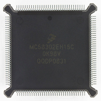
IC MPU MULTI-PROTOCOL 132-PQFP
Manufacturer
Freescale Semiconductor
Datasheets
1.MC68302AG20C.pdf
(4 pages)
2.MC68302AG20C.pdf
(2 pages)
3.MC68302AG20C.pdf
(13 pages)
4.MC68302EH16C.pdf
(481 pages)
Specifications of MC68302EH16C
Processor Type
M683xx 32-Bit
Speed
16MHz
Voltage
5V
Mounting Type
Surface Mount
Package / Case
132-MQFP, 132-PQFP
Controller Family/series
68K
Core Size
32 Bit
Ram Memory Size
1152Byte
Cpu Speed
16MHz
No. Of Timers
3
Embedded Interface Type
SCP, TDM
Digital Ic Case Style
PQFP
Rohs Compliant
Yes
Family Name
M68000
Device Core
ColdFire
Device Core Size
32b
Frequency (max)
16MHz
Instruction Set Architecture
RISC
Supply Voltage 1 (typ)
5V
Operating Temp Range
0C to 70C
Operating Temperature Classification
Commercial
Mounting
Surface Mount
Pin Count
132
Package Type
PQFP
Lead Free Status / RoHS Status
Lead free / RoHS Compliant
Features
-
Lead Free Status / Rohs Status
RoHS Compliant part
Electrostatic Device
Available stocks
Company
Part Number
Manufacturer
Quantity
Price
Company:

Part Number:
MC68302EH16C
Manufacturer:
Freescale Semiconductor
Quantity:
135
Company:
Part Number:
MC68302EH16C
Manufacturer:
PANA
Quantity:
99
Company:
Part Number:
MC68302EH16C
Manufacturer:
Freescale Semiconductor
Quantity:
10 000
Part Number:
MC68302EH16C
Manufacturer:
FREESCALE
Quantity:
20 000
Company:
Part Number:
MC68302EH16CB1
Manufacturer:
Freescale Semiconductor
Quantity:
10 000
Company:
Part Number:
MC68302EH16CR2
Manufacturer:
Freescale Semiconductor
Quantity:
10 000


OFFSET + 0
OFFSET + 2
OFFSET + 4
ENC—Data Encoding Format
COMMON SCC MODE BITS—See 4.5.3 SCC Mode Register (SCM) for a description of the
DIAG1, DIAG0, ENR, ENT, MODE1, and MODE0 bits.
4.5.12.10 HDLC Receive Buffer Descriptor (Rx BD)
The HDLC controller uses the Rx BD to report information about the received data for each
buffer. The Rx BD is shown in Figure 4-26.
OFFSET +6
An example of the HDLC receive process is shown in Figure 4-27. This shows the resulting
state of the Rx BDs after receipt of a complete frame spanning two receive buffers and a
second frame with an unexpected abort sequence. The example assumes that MRBLR = 8
in the SCC parameter RAM.
The first word of the Rx BD contains control and status bits. Bits 15–10 are written by the
user before the buffer is linked to the Rx BD table, and bits 5–0 are set by the CP following
frame reception. Bit 15 is set by the M68000 core when the buffer is available to the HDLC
controller; it is cleared by the HDLC controller when the buffer is full.
E—Empty
X—External Buffer
MOTOROLA
0 = Non-return to zero (NRZ). A one is a high level; a zero is a low level.
1 = Non-return to zero inverted (NRZI). A one is represented by no change in the level;
0 = The data buffer associated with this BD has been filled with received data, or data
1 = The data buffer associated with the BD is empty. This bit signifies that the BD and
0 = The buffer associated with this BD is in internal dual-port RAM.
1 = The buffer associated with this BD is in external memory.
a zero is represented by a change in the level. The receiver decodes NRZI, but a
clock must be supplied. The transmitter encodes NRZI. During an idle condition,
with the FLG bit cleared, the line will be forced to a high state.
reception has been aborted due to an error condition. The M68000 core is free to
examine or write to any fields of the BD.
its associated buffer are available to the HDLC controller. The M68000 core should
not write to any fields of this BD after it sets this bit. The empty bit will remain set
while the HDLC controller is currently filling the buffer with received data.
15
E
14
X
Figure 4-26. HDLC Receive Buffer Descriptor
13
W
12
I
RX BUFFER POINTER (24-bits used, upper 8 bits must be 0)
11
L
MC68302 USER’S MANUAL
10
F
—
9
DATA LENGTH
—
8
—
7
—
6
Communications Processor (CP)
LG
5
NO
4
AB
3
CR
2
OV
1
4-75
CD
0
Related parts for MC68302EH16C
Image
Part Number
Description
Manufacturer
Datasheet
Request
R

Part Number:
Description:
Manufacturer:
Freescale Semiconductor, Inc
Datasheet:

Part Number:
Description:
MC68302 Configuring the Chip Selects on the MC68302
Manufacturer:
Motorola / Freescale Semiconductor
Part Number:
Description:
MC68302 Design Concept - Expanding Interrupts on the MC68302
Manufacturer:
Motorola / Freescale Semiconductor
Part Number:
Description:
MC68302 MC68302 Adapting a WAN Controller to a LAN Environment
Manufacturer:
Motorola / Freescale Semiconductor
Part Number:
Description:
MC68302 EKB Applications - Power Measurements on the MC68302
Manufacturer:
Motorola / Freescale Semiconductor
Part Number:
Description:
MC68302 Interfacing the MC68020 to a Slave MC68302
Manufacturer:
Motorola / Freescale Semiconductor
Part Number:
Description:
MC68302 MC68302 Software Performance
Manufacturer:
Motorola / Freescale Semiconductor
Part Number:
Description:
MC68302 Evaluating EDX on the ADS302
Manufacturer:
Motorola / Freescale Semiconductor
Part Number:
Description:
MC68302 Design Advisory #1 - MC68SC302 Passive ISDN Protocol Engine
Manufacturer:
Motorola / Freescale Semiconductor
Part Number:
Description:
MC68302, MC68360, and MPC860 Characteristics and Design Notes for Crystal Feedback Oscillators
Manufacturer:
Motorola / Freescale Semiconductor
Part Number:
Description:
Mc68302 Integrated Multi-protocol Processor
Manufacturer:
Freescale Semiconductor, Inc
Datasheet:
Part Number:
Description:
Manufacturer:
Freescale Semiconductor, Inc
Datasheet:
Part Number:
Description:
Manufacturer:
Freescale Semiconductor, Inc
Datasheet:
Part Number:
Description:
Manufacturer:
Freescale Semiconductor, Inc
Datasheet:
Part Number:
Description:
Manufacturer:
Freescale Semiconductor, Inc
Datasheet: