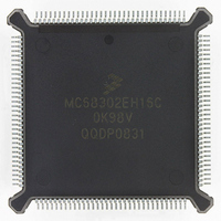
MC68302EH16C Freescale Semiconductor, MC68302EH16C Datasheet - Page 407

MC68302EH16C
Manufacturer Part Number
MC68302EH16C
Description
IC MPU MULTI-PROTOCOL 132-PQFP
Manufacturer
Freescale Semiconductor
Datasheets
1.MC68302AG20C.pdf
(4 pages)
2.MC68302AG20C.pdf
(2 pages)
3.MC68302AG20C.pdf
(13 pages)
4.MC68302EH16C.pdf
(481 pages)
Specifications of MC68302EH16C
Processor Type
M683xx 32-Bit
Speed
16MHz
Voltage
5V
Mounting Type
Surface Mount
Package / Case
132-MQFP, 132-PQFP
Controller Family/series
68K
Core Size
32 Bit
Ram Memory Size
1152Byte
Cpu Speed
16MHz
No. Of Timers
3
Embedded Interface Type
SCP, TDM
Digital Ic Case Style
PQFP
Rohs Compliant
Yes
Family Name
M68000
Device Core
ColdFire
Device Core Size
32b
Frequency (max)
16MHz
Instruction Set Architecture
RISC
Supply Voltage 1 (typ)
5V
Operating Temp Range
0C to 70C
Operating Temperature Classification
Commercial
Mounting
Surface Mount
Pin Count
132
Package Type
PQFP
Lead Free Status / RoHS Status
Lead free / RoHS Compliant
Features
-
Lead Free Status / Rohs Status
RoHS Compliant part
Electrostatic Device
Available stocks
Company
Part Number
Manufacturer
Quantity
Price
Company:
Part Number:
MC68302EH16C
Manufacturer:
Freescale Semiconductor
Quantity:
135
Company:
Part Number:
MC68302EH16C
Manufacturer:
PANA
Quantity:
99
Company:
Part Number:
MC68302EH16C
Manufacturer:
Freescale Semiconductor
Quantity:
10 000
Part Number:
MC68302EH16C
Manufacturer:
FREESCALE
Quantity:
20 000
Company:
Part Number:
MC68302EH16CB1
Manufacturer:
Freescale Semiconductor
Quantity:
10 000
Company:
Part Number:
MC68302EH16CR2
Manufacturer:
Freescale Semiconductor
Quantity:
10 000
- MC68302AG20C PDF datasheet
- MC68302AG20C PDF datasheet #2
- MC68302AG20C PDF datasheet #3
- MC68302EH16C PDF datasheet #4
- Current page: 407 of 481
- Download datasheet (2Mb)
For instance, you could create a protocol that sends and receives the following:
syn-syn-Data-Data-ETX-syn-syn-syn-syn-Data-ETX-syn-syn
where syn is a defined one-byte sync character, ETX is the one-byte control character on
which to close the receive buffer (BISYNC terminology), and data is any other byte value.
On reception, the first three bytes can be stored in one receive buffer, and the next two bytes
can be stored in a different receive buffer (ETX is not discarded from the receive buffer). The
receiver in BISYNC mode will strip the syn bytes and use the ETX character to generate a
control character interrupt to close the current receive buffer. Thus, data bytes must not con-
tain syn or ETX characters!
On transmission, the first three bytes may be stored in one transmit buffer and the next two
bytes in the next transmit buffer. At least two sync characters must be transmitted before
every frame. If the next buffer is not ready immediately, additional syncs will be inserted (as
shown in the preceding example by two extra syncs (for a total of four) between the two
frames). If the transmitter underruns, the syn character will be inserted. One advantage of
this BlSYNC-type configuration is that an underrun is not fatal and has no effect on reception
of correct data.
Assuming that syn = $45 and ETX = $44, registers should be set up as follows for a loopback
test of BISYNC mode:
Other registers, such as MRBLR, RFCR, TFCR, SCCM, IMR, and SIMODE, still have to be
defined, but their values are of no particular relevance to the loopback operation.
MOTOROLA
DSR = $4545—This register contains a pair of sync characters. In this register, they are
termed SYN1-SYN2. They do not have to be the same byte repeated twice, although
there is no particular advantage in using different bytes. Since any characters can be used
as the sync characters, it is even possible to choose HDLC flags ($7E7E) if desired.
SCM = $089F—This setting selects normal BISYNC, loopback enabled, BCS disabled,
and transmit SYN1-SYN2 pairs between frames. It is also possible to transmit ones be-
tween frames instead of SYN1-SYN2, but a sync character must be included at the end
of each transmit buffer to ensure that the receiver sees a sync at the end of the frame.
BSYNC = $8045—This defines the underrun sync on the transmit side and ensures the
receiver will not put the sync in the receive buffer.
BDLE = $00ff—Disables the BISYNC DLE function.
PRCRC, PTCRC = $0000—It is good practice to clear these even though they are not
used.
Control Char Table Entry 1 = $2044—Closes the receive buffer upon reception of an ETX
character.
Control Char Table Entry 2 = $8000—This setting disables control char table
entries 2-8.
Note that the preceding list of registers is not meant to suggest that these registers should
be written in this order. Refer to 4.5.7 SCC Initialization for the proper order.
MC68302 USER’S MANUAL
MC68302 Applications
D-57
Related parts for MC68302EH16C
Image
Part Number
Description
Manufacturer
Datasheet
Request
R
Part Number:
Description:
Manufacturer:
Freescale Semiconductor, Inc
Datasheet:

Part Number:
Description:
MC68302 Configuring the Chip Selects on the MC68302
Manufacturer:
Motorola / Freescale Semiconductor

Part Number:
Description:
MC68302 Design Concept - Expanding Interrupts on the MC68302
Manufacturer:
Motorola / Freescale Semiconductor

Part Number:
Description:
MC68302 MC68302 Adapting a WAN Controller to a LAN Environment
Manufacturer:
Motorola / Freescale Semiconductor

Part Number:
Description:
MC68302 EKB Applications - Power Measurements on the MC68302
Manufacturer:
Motorola / Freescale Semiconductor

Part Number:
Description:
MC68302 Interfacing the MC68020 to a Slave MC68302
Manufacturer:
Motorola / Freescale Semiconductor

Part Number:
Description:
MC68302 MC68302 Software Performance
Manufacturer:
Motorola / Freescale Semiconductor

Part Number:
Description:
MC68302 Evaluating EDX on the ADS302
Manufacturer:
Motorola / Freescale Semiconductor

Part Number:
Description:
MC68302 Design Advisory #1 - MC68SC302 Passive ISDN Protocol Engine
Manufacturer:
Motorola / Freescale Semiconductor

Part Number:
Description:
MC68302, MC68360, and MPC860 Characteristics and Design Notes for Crystal Feedback Oscillators
Manufacturer:
Motorola / Freescale Semiconductor
Part Number:
Description:
Mc68302 Integrated Multi-protocol Processor
Manufacturer:
Freescale Semiconductor, Inc
Datasheet:
Part Number:
Description:
Manufacturer:
Freescale Semiconductor, Inc
Datasheet:
Part Number:
Description:
Manufacturer:
Freescale Semiconductor, Inc
Datasheet:
Part Number:
Description:
Manufacturer:
Freescale Semiconductor, Inc
Datasheet:
Part Number:
Description:
Manufacturer:
Freescale Semiconductor, Inc
Datasheet:


