MC68302EH16C Freescale Semiconductor, MC68302EH16C Datasheet - Page 356
MC68302EH16C
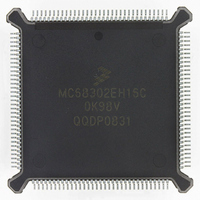
Manufacturer Part Number
MC68302EH16C
Description
IC MPU MULTI-PROTOCOL 132-PQFP
Manufacturer
Freescale Semiconductor
Datasheets
1.MC68302AG20C.pdf
(4 pages)
2.MC68302AG20C.pdf
(2 pages)
3.MC68302AG20C.pdf
(13 pages)
4.MC68302EH16C.pdf
(481 pages)
Specifications of MC68302EH16C
Processor Type
M683xx 32-Bit
Speed
16MHz
Voltage
5V
Mounting Type
Surface Mount
Package / Case
132-MQFP, 132-PQFP
Controller Family/series
68K
Core Size
32 Bit
Ram Memory Size
1152Byte
Cpu Speed
16MHz
No. Of Timers
3
Embedded Interface Type
SCP, TDM
Digital Ic Case Style
PQFP
Rohs Compliant
Yes
Family Name
M68000
Device Core
ColdFire
Device Core Size
32b
Frequency (max)
16MHz
Instruction Set Architecture
RISC
Supply Voltage 1 (typ)
5V
Operating Temp Range
0C to 70C
Operating Temperature Classification
Commercial
Mounting
Surface Mount
Pin Count
132
Package Type
PQFP
Lead Free Status / RoHS Status
Lead free / RoHS Compliant
Features
-
Lead Free Status / Rohs Status
RoHS Compliant part
Electrostatic Device
Available stocks
Company
Part Number
Manufacturer
Quantity
Price
Company:

Part Number:
MC68302EH16C
Manufacturer:
Freescale Semiconductor
Quantity:
135
Company:
Part Number:
MC68302EH16C
Manufacturer:
PANA
Quantity:
99
Company:
Part Number:
MC68302EH16C
Manufacturer:
Freescale Semiconductor
Quantity:
10 000
Part Number:
MC68302EH16C
Manufacturer:
FREESCALE
Quantity:
20 000
Company:
Part Number:
MC68302EH16CB1
Manufacturer:
Freescale Semiconductor
Quantity:
10 000
Company:
Part Number:
MC68302EH16CR2
Manufacturer:
Freescale Semiconductor
Quantity:
10 000


MC68302 Applications
ing this register, the compare function code (CFC) bit should be cleared, since data stored
in the program ROM will need to be accessed and moved to other areas of memory. (At re-
set, the function code for CS0 defaults to 110b to select supervisor program, and the func-
tion code comparison is enabled). Thus, OR0 could be written with $5F80 for this example.
Next, the RAM addresses should be defined. To set the range of the RAM for 64 kbytes, to
configure it for zero wait states, to allow both reads and writes, and to disable function code
comparisons, OR1 should be set to $1FE0. To initially place the RAM at $400000, enable
the RAM and set the function code to supervisor data; BR1 should be set to $A801.
Now that the RAM is enabled, an initial set of vectors may be placed in it (i.e., copied from
the ROM). Of course, they will not be accessed as vectors until the RAM is moved to location
0. Any exceptions that occur during this time will still have their vectors derived from the
ROM vector table.
The following situation now exists:
D.2.3 Switching Process
To perform the switch, jump from the ROM to the dual-port RAM, reconfigure chip selects 1
and 0, and then jump back to the ROM. It is important that the RAM be moved first to ensure
that an exception vector table is always present. During the brief period while the locations
in CS1 and CS0 overlap, CS0 will take precedence.
To perform the switch we need to execute a short dual-port RAM program. Thus, we copy
the following data (instructions) from ROM to the dual-port RAM starting at location
$700000:
Thus, first copy the binary coding of the preceding program from ROM to the dual-port RAM
starting at location $700000.
Next, execute
which then causes the following final situation:
The initialization of chip selects 0 and 1 and the switch of ROM and RAM are now complete.
D-6
ROM—$0 to $03FFFF
RAM—$400000 to $40FFFF
MC68302—$700000 to $700FFF
RAM—$000000 to $00FFFF
ROM—$100000 to $13FFFF
MC68302—$700000 to $700FFF
MOVE.W
MOVE.W
JMP
JMP
($700000).L
($Address in ROM).L
#$A001, ($700834).L
#$C201, ($700830).L
MC68302 USER’S MANUAL
; Place CS1 at $0 by writing to BR1
; Place CS0 at $100000 by writing to BR0
; Jump to Dual-Port RAM
MOTOROLA
Related parts for MC68302EH16C
Image
Part Number
Description
Manufacturer
Datasheet
Request
R

Part Number:
Description:
Manufacturer:
Freescale Semiconductor, Inc
Datasheet:

Part Number:
Description:
MC68302 Configuring the Chip Selects on the MC68302
Manufacturer:
Motorola / Freescale Semiconductor
Part Number:
Description:
MC68302 Design Concept - Expanding Interrupts on the MC68302
Manufacturer:
Motorola / Freescale Semiconductor
Part Number:
Description:
MC68302 MC68302 Adapting a WAN Controller to a LAN Environment
Manufacturer:
Motorola / Freescale Semiconductor
Part Number:
Description:
MC68302 EKB Applications - Power Measurements on the MC68302
Manufacturer:
Motorola / Freescale Semiconductor
Part Number:
Description:
MC68302 Interfacing the MC68020 to a Slave MC68302
Manufacturer:
Motorola / Freescale Semiconductor
Part Number:
Description:
MC68302 MC68302 Software Performance
Manufacturer:
Motorola / Freescale Semiconductor
Part Number:
Description:
MC68302 Evaluating EDX on the ADS302
Manufacturer:
Motorola / Freescale Semiconductor
Part Number:
Description:
MC68302 Design Advisory #1 - MC68SC302 Passive ISDN Protocol Engine
Manufacturer:
Motorola / Freescale Semiconductor
Part Number:
Description:
MC68302, MC68360, and MPC860 Characteristics and Design Notes for Crystal Feedback Oscillators
Manufacturer:
Motorola / Freescale Semiconductor
Part Number:
Description:
Mc68302 Integrated Multi-protocol Processor
Manufacturer:
Freescale Semiconductor, Inc
Datasheet:
Part Number:
Description:
Manufacturer:
Freescale Semiconductor, Inc
Datasheet:
Part Number:
Description:
Manufacturer:
Freescale Semiconductor, Inc
Datasheet:
Part Number:
Description:
Manufacturer:
Freescale Semiconductor, Inc
Datasheet:
Part Number:
Description:
Manufacturer:
Freescale Semiconductor, Inc
Datasheet: