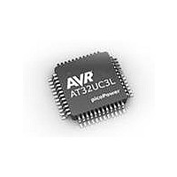
AT32UC3L032-D3UR Atmel, AT32UC3L032-D3UR Datasheet - Page 11

AT32UC3L032-D3UR
Manufacturer Part Number
AT32UC3L032-D3UR
Description
MCU AVR32 32KB FLASH 48TLLGA
Manufacturer
Atmel
Series
AVR®32 UC3r
Datasheet
1.AT32UC3L-EK.pdf
(858 pages)
Specifications of AT32UC3L032-D3UR
Core Processor
AVR
Core Size
32-Bit
Speed
50MHz
Connectivity
I²C, SPI, UART/USART
Peripherals
Brown-out Detect/Reset, DMA, PWM, WDT
Number Of I /o
36
Program Memory Size
32KB (32K x 8)
Program Memory Type
FLASH
Ram Size
16K x 8
Voltage - Supply (vcc/vdd)
1.62 V ~ 3.6 V
Data Converters
A/D 9x10b
Oscillator Type
Internal
Operating Temperature
-40°C ~ 85°C
Package / Case
48-TLLGA
Processor Series
AT32UC3x
Core
AVR32
Data Bus Width
32 bit
Data Ram Size
16 KB
Interface Type
SPI, TWI, USART
Maximum Clock Frequency
50 MHz
Number Of Programmable I/os
36
Number Of Timers
7
Maximum Operating Temperature
+ 85 C
Mounting Style
SMD/SMT
3rd Party Development Tools
EWAVR32, EWAVR32-BL
Development Tools By Supplier
AT32UC3L-EK
Minimum Operating Temperature
- 40 C
On-chip Adc
10 bit, 9 Channel
Lead Free Status / RoHS Status
Lead free / RoHS Compliant
Eeprom Size
-
Lead Free Status / Rohs Status
Details
- Current page: 11 of 858
- Download datasheet (13Mb)
3.2.2
3.2.3
3.2.4
32099F–11/2010
Peripheral Functions
JTAG Port Connections
Nexus OCD AUX Port Connections
Refer to the
ties of the TWI, 5V Tolerant, and SMBUS pins.
Each GPIO line can be assigned to one of several peripheral functions. The following table
describes how the various peripheral functions are selected. The last listed function has priority
in case multiple functions are enabled on the same pin.
Table 3-2.
If the JTAG is enabled, the JTAG will take control over a number of pins, irrespectively of the I/O
Controller configuration.
Table 3-3.
If the OCD trace system is enabled, the trace system will take control over a number of pins, irre-
spectively of the I/O Controller configuration. Two different OCD trace pin mappings are
possible, depending on the configuration of the OCD AXS register. For details, see the AVR32
UC Technical Reference Manual.
Table 3-4.
Function
GPIO Controller Function multiplexing
Nexus OCD AUX port connections
aWire DATAOUT
JTAG port connections
Oscillators
Pin
EVTI_N
MDO[5]
MDO[4]
MDO[3]
”TWI Pin Characteristics(1)” on page 790
48-pin
Peripheral Functions
JTAG Pinout
Nexus OCD AUX Port Connections
11
14
13
4
AXS=1
PA05
PA10
PA18
PA17
AXS=0
PB08
PB00
PB04
PB05
Description
GPIO and GPIO peripheral selection A to H
OCD trace system
aWire output in two-pin mode
JTAG debug port
OSC0, OSC32
Pin Name
PA00
PA01
PA02
PA03
for a description of the electrical proper-
AT32UC3L016/32/64
JTAG Pin
TMS
TDO
TCK
TDI
11
Related parts for AT32UC3L032-D3UR
Image
Part Number
Description
Manufacturer
Datasheet
Request
R

Part Number:
Description:
KIT DEV/EVAL FOR AT32UC3L0
Manufacturer:
Atmel
Datasheet:

Part Number:
Description:
DEV KIT FOR AVR/AVR32
Manufacturer:
Atmel
Datasheet:

Part Number:
Description:
INTERVAL AND WIPE/WASH WIPER CONTROL IC WITH DELAY
Manufacturer:
ATMEL Corporation
Datasheet:

Part Number:
Description:
Low-Voltage Voice-Switched IC for Hands-Free Operation
Manufacturer:
ATMEL Corporation
Datasheet:

Part Number:
Description:
MONOLITHIC INTEGRATED FEATUREPHONE CIRCUIT
Manufacturer:
ATMEL Corporation
Datasheet:

Part Number:
Description:
AM-FM Receiver IC U4255BM-M
Manufacturer:
ATMEL Corporation
Datasheet:

Part Number:
Description:
Monolithic Integrated Feature Phone Circuit
Manufacturer:
ATMEL Corporation
Datasheet:

Part Number:
Description:
Multistandard Video-IF and Quasi Parallel Sound Processing
Manufacturer:
ATMEL Corporation
Datasheet:

Part Number:
Description:
High-performance EE PLD
Manufacturer:
ATMEL Corporation
Datasheet:

Part Number:
Description:
8-bit Flash Microcontroller
Manufacturer:
ATMEL Corporation
Datasheet:

Part Number:
Description:
2-Wire Serial EEPROM
Manufacturer:
ATMEL Corporation
Datasheet:


