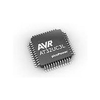
AT32UC3L032-D3UR Atmel, AT32UC3L032-D3UR Datasheet - Page 608

AT32UC3L032-D3UR
Manufacturer Part Number
AT32UC3L032-D3UR
Description
MCU AVR32 32KB FLASH 48TLLGA
Manufacturer
Atmel
Series
AVR®32 UC3r
Datasheet
1.AT32UC3L-EK.pdf
(858 pages)
Specifications of AT32UC3L032-D3UR
Core Processor
AVR
Core Size
32-Bit
Speed
50MHz
Connectivity
I²C, SPI, UART/USART
Peripherals
Brown-out Detect/Reset, DMA, PWM, WDT
Number Of I /o
36
Program Memory Size
32KB (32K x 8)
Program Memory Type
FLASH
Ram Size
16K x 8
Voltage - Supply (vcc/vdd)
1.62 V ~ 3.6 V
Data Converters
A/D 9x10b
Oscillator Type
Internal
Operating Temperature
-40°C ~ 85°C
Package / Case
48-TLLGA
Processor Series
AT32UC3x
Core
AVR32
Data Bus Width
32 bit
Data Ram Size
16 KB
Interface Type
SPI, TWI, USART
Maximum Clock Frequency
50 MHz
Number Of Programmable I/os
36
Number Of Timers
7
Maximum Operating Temperature
+ 85 C
Mounting Style
SMD/SMT
3rd Party Development Tools
EWAVR32, EWAVR32-BL
Development Tools By Supplier
AT32UC3L-EK
Minimum Operating Temperature
- 40 C
On-chip Adc
10 bit, 9 Channel
Lead Free Status / RoHS Status
Lead free / RoHS Compliant
Eeprom Size
-
Lead Free Status / Rohs Status
Details
- Current page: 608 of 858
- Download datasheet (13Mb)
26.7.3
32099F–11/2010
Resistive Touch Screen Pin Connections
In an ideal world (linear, with no loss), the vertical position is equal to:
To compensate for some of the real world imperfections, VX
used to improve accuracy at the cost of two more conversions per axes. The new expression for
the vertical position then becomes:
Table 26-2.
The resistive touch screen film signals connects to the ADCIFB using the AD and ADP pins. The
X
(right) and Y
configurable through the Touch Screen Pin Offset (TSPO) field in the Mode Register (MR) and
allows the user to configure which AD pins to use for resistive touch screen applications. Writing
a zero to the TSPO field instructs the ADCIFB to use AD0 through AD3, where AD0 is con-
nected to X
ADCIFB to use AD1 through AD4 for resistive touch screen sequencing, where AD1 is con-
nected to X
When the Analog Pin Output Enable (APOE) bit in the Mode Register (MR) is zero, the AD pins
are used to measure input voltage and drive the GND sequences, while the ADP pins are used
to drive the VDD sequences. This arrangement allows the user to reduce the voltage seen at the
AD input pins by inserting external resistors between ADP0 and X
which are again directly connected to the AD pins. It is important that the voltages observed at
the AD pins are not higher than the maximum allowed ADC input voltage. See
page 610
ADP pins.
By adding a resistor between ADP0 and X
at the AD pins can be controlled by the following voltage divider expressions:
The Rfilmx parameter is the film resistance observed when measuring between X
Rresistorx parameter is the resistor size inserted between ADP0 and X
and Rresistory is the same but for ADP1, Y
ADCIFB Pin
ADP0
ADP1
ADtspo+0
ADtspo+1
ADtspo+2
ADtspo+3
P
(top) and X
VY
(VY
P
P
for details regarding how to connect the resistive touch screen films to the AD and
/ VDD
P
- VX
P
M
, AD1 is connected to X
and AD0 is free to be used as an ordinary ADC channel.
M
Resistive Touch Screen Pin Connections
(left) signals are connected to ADtspo+2 and ADtspo+3 pins. The tspo index is
M
(bottom) film signals are connected to ADtspo+0 and ADtspo+1 pins, and the Y
) / (VX
P
- VX
M
)
TS Signal, APOE == 0
Xp through a resistor
Yp through a resistor
Xp
Xm
Yp
Ym
M
and so on. Writing a one to the TSPO field instructs the
P
P
, and ADP1 and Y
, and Y
M
instead.
AT32UC3L016/32/64
P
P
, the maximum voltage observed
and VX
No Connect
No Connect
TS Signal, APOE == 1
Xp
Xm
Yp
Ym
P
and ADP1 and Y
P
m
. The definition of Rfilmy
can be measured and
Figure 26-3 on
P
and X
P
signals
M
. The
608
P
Related parts for AT32UC3L032-D3UR
Image
Part Number
Description
Manufacturer
Datasheet
Request
R

Part Number:
Description:
KIT DEV/EVAL FOR AT32UC3L0
Manufacturer:
Atmel
Datasheet:

Part Number:
Description:
DEV KIT FOR AVR/AVR32
Manufacturer:
Atmel
Datasheet:

Part Number:
Description:
INTERVAL AND WIPE/WASH WIPER CONTROL IC WITH DELAY
Manufacturer:
ATMEL Corporation
Datasheet:

Part Number:
Description:
Low-Voltage Voice-Switched IC for Hands-Free Operation
Manufacturer:
ATMEL Corporation
Datasheet:

Part Number:
Description:
MONOLITHIC INTEGRATED FEATUREPHONE CIRCUIT
Manufacturer:
ATMEL Corporation
Datasheet:

Part Number:
Description:
AM-FM Receiver IC U4255BM-M
Manufacturer:
ATMEL Corporation
Datasheet:

Part Number:
Description:
Monolithic Integrated Feature Phone Circuit
Manufacturer:
ATMEL Corporation
Datasheet:

Part Number:
Description:
Multistandard Video-IF and Quasi Parallel Sound Processing
Manufacturer:
ATMEL Corporation
Datasheet:

Part Number:
Description:
High-performance EE PLD
Manufacturer:
ATMEL Corporation
Datasheet:

Part Number:
Description:
8-bit Flash Microcontroller
Manufacturer:
ATMEL Corporation
Datasheet:

Part Number:
Description:
2-Wire Serial EEPROM
Manufacturer:
ATMEL Corporation
Datasheet:


