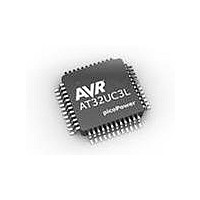
AT32UC3L032-D3UR Atmel, AT32UC3L032-D3UR Datasheet - Page 330

AT32UC3L032-D3UR
Manufacturer Part Number
AT32UC3L032-D3UR
Description
MCU AVR32 32KB FLASH 48TLLGA
Manufacturer
Atmel
Series
AVR®32 UC3r
Datasheet
1.AT32UC3L-EK.pdf
(858 pages)
Specifications of AT32UC3L032-D3UR
Core Processor
AVR
Core Size
32-Bit
Speed
50MHz
Connectivity
I²C, SPI, UART/USART
Peripherals
Brown-out Detect/Reset, DMA, PWM, WDT
Number Of I /o
36
Program Memory Size
32KB (32K x 8)
Program Memory Type
FLASH
Ram Size
16K x 8
Voltage - Supply (vcc/vdd)
1.62 V ~ 3.6 V
Data Converters
A/D 9x10b
Oscillator Type
Internal
Operating Temperature
-40°C ~ 85°C
Package / Case
48-TLLGA
Processor Series
AT32UC3x
Core
AVR32
Data Bus Width
32 bit
Data Ram Size
16 KB
Interface Type
SPI, TWI, USART
Maximum Clock Frequency
50 MHz
Number Of Programmable I/os
36
Number Of Timers
7
Maximum Operating Temperature
+ 85 C
Mounting Style
SMD/SMT
3rd Party Development Tools
EWAVR32, EWAVR32-BL
Development Tools By Supplier
AT32UC3L-EK
Minimum Operating Temperature
- 40 C
On-chip Adc
10 bit, 9 Channel
Lead Free Status / RoHS Status
Lead free / RoHS Compliant
Eeprom Size
-
Lead Free Status / Rohs Status
Details
- Current page: 330 of 858
- Download datasheet (13Mb)
18.6.2
18.6.2.1
18.6.2.2
18.6.2.3
18.6.2.4
32099F–11/2010
Advanced Operation
Peripheral I/O Pin Control
Pull-up Resistor Control
Output Pin Timings
Interrupts
When a GPIO pin is assigned to a peripheral function, i.e. the corresponding bit in GPER is zero,
output and output enable is controlled by the selected peripheral pin. In addition the peripheral
may control some or all of the other GPIO pin functions listed in
ports those features. All pin features not controlled by the selected peripheral is controlled by the
GPIO.
Refer to the Module Configuration section for details regarding implemented GPIO pin functions
and to the Peripheral chapter for details regarding I/O pin function control.
Table 18-1.
Pull-up can be configured for each GPIO pin. Pull-up allows the pin and any connected net to be
pulled up to VDD if the net is not driven.
Pull-up is useful for detecting if a pin is unconnected or if a mechanical button is pressed, for var-
ious communication protocols and to keep unconnected pins from floating.
Pull-up can be enabled and disabled by writing a one and a zero respectively to the correspond-
ing bit in the Pull-up Enable Register (PUER).
Figure 18-3
The same timing applies when performing a ‘set’ or ‘clear’ access, i.e. writing to OVRS or
OVRC. The timing of PVR is also shown.
Figure 18-3. Output Pin Timings
The GPIO can be configured to generate an interrupt when it detects a change on a GPIO pin.
Interrupts on a pin are enabled by writing a one to the corresponding bit in the Interrupt Enable
Function name
Output
Output enable
Pull-up
Write OVR to 1
Write OVR to 0
OVR / I/O Line
CLK_GPIO
PVR
shows the timing of the GPIO pin when writing to the Output Value Register (OVR).
I/O Pin function Control
GPIO mode
OVR
ODER
PUER
PB Access
Peripheral mode
Peripheral
Peripheral
Peripheral if supported, else GPIO
AT32UC3L016/32/64
PB Access
Table
18-1, if the peripheral sup-
330
Related parts for AT32UC3L032-D3UR
Image
Part Number
Description
Manufacturer
Datasheet
Request
R

Part Number:
Description:
KIT DEV/EVAL FOR AT32UC3L0
Manufacturer:
Atmel
Datasheet:

Part Number:
Description:
DEV KIT FOR AVR/AVR32
Manufacturer:
Atmel
Datasheet:

Part Number:
Description:
INTERVAL AND WIPE/WASH WIPER CONTROL IC WITH DELAY
Manufacturer:
ATMEL Corporation
Datasheet:

Part Number:
Description:
Low-Voltage Voice-Switched IC for Hands-Free Operation
Manufacturer:
ATMEL Corporation
Datasheet:

Part Number:
Description:
MONOLITHIC INTEGRATED FEATUREPHONE CIRCUIT
Manufacturer:
ATMEL Corporation
Datasheet:

Part Number:
Description:
AM-FM Receiver IC U4255BM-M
Manufacturer:
ATMEL Corporation
Datasheet:

Part Number:
Description:
Monolithic Integrated Feature Phone Circuit
Manufacturer:
ATMEL Corporation
Datasheet:

Part Number:
Description:
Multistandard Video-IF and Quasi Parallel Sound Processing
Manufacturer:
ATMEL Corporation
Datasheet:

Part Number:
Description:
High-performance EE PLD
Manufacturer:
ATMEL Corporation
Datasheet:

Part Number:
Description:
8-bit Flash Microcontroller
Manufacturer:
ATMEL Corporation
Datasheet:

Part Number:
Description:
2-Wire Serial EEPROM
Manufacturer:
ATMEL Corporation
Datasheet:


