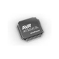
AT32UC3L032-D3UR Atmel, AT32UC3L032-D3UR Datasheet - Page 759

AT32UC3L032-D3UR
Manufacturer Part Number
AT32UC3L032-D3UR
Description
MCU AVR32 32KB FLASH 48TLLGA
Manufacturer
Atmel
Series
AVR®32 UC3r
Datasheet
1.AT32UC3L-EK.pdf
(858 pages)
Specifications of AT32UC3L032-D3UR
Core Processor
AVR
Core Size
32-Bit
Speed
50MHz
Connectivity
I²C, SPI, UART/USART
Peripherals
Brown-out Detect/Reset, DMA, PWM, WDT
Number Of I /o
36
Program Memory Size
32KB (32K x 8)
Program Memory Type
FLASH
Ram Size
16K x 8
Voltage - Supply (vcc/vdd)
1.62 V ~ 3.6 V
Data Converters
A/D 9x10b
Oscillator Type
Internal
Operating Temperature
-40°C ~ 85°C
Package / Case
48-TLLGA
Processor Series
AT32UC3x
Core
AVR32
Data Bus Width
32 bit
Data Ram Size
16 KB
Interface Type
SPI, TWI, USART
Maximum Clock Frequency
50 MHz
Number Of Programmable I/os
36
Number Of Timers
7
Maximum Operating Temperature
+ 85 C
Mounting Style
SMD/SMT
3rd Party Development Tools
EWAVR32, EWAVR32-BL
Development Tools By Supplier
AT32UC3L-EK
Minimum Operating Temperature
- 40 C
On-chip Adc
10 bit, 9 Channel
Lead Free Status / RoHS Status
Lead free / RoHS Compliant
Eeprom Size
-
Lead Free Status / Rohs Status
Details
- Current page: 759 of 858
- Download datasheet (13Mb)
31.5.3.6
31.5.3.7
32099F–11/2010
CANCEL_ACCESS
SYNC
Table 31-23. MEMORY_BLOCK_ACCESS Details (Continued)
The overhead using block word access is 4 cycles per 32 bits of data, resulting in an 88% trans-
fer efficiency, or 2.1 MBytes per second with a 20 MHz TCK frequency.
If a very slow memory location is accessed during a SAB memory access, it could take a very
long time until the busy bit is cleared, and the SAB becomes ready for the next operation. The
CANCEL_ACCESS instruction provides a possibility to abort an ongoing transfer and report a
timeout to the JTAG master.
When the CANCEL_ACCESS instruction is selected, the current access will be terminated as
soon as possible. There are no guarantees about how long this will take, as the hardware may
not always be able to cancel the access immediately. The SAB is ready to respond to a new
command when the busy bit clears.
Starting in Run-Test/Idle, CANCEL_ACCESS is accessed in the following way:
Table 31-24. CANCEL_ACCESS Details
This instruction allows external debuggers and testers to measure the ratio between the external
JTAG clock and the internal system clock. The SYNC data register is a 16-bit counter that
counts down to zero using the internal system clock. The busy bit stays high until the counter
reaches zero.
Starting in Run-Test/Idle, SYNC instruction is used in the following way:
Instructions
DR input value (Data write phase)
DR output value (Data read phase)
DR output value (Data write phase)
Instructions
IR input value
IR output value
DR Size
DR input value
DR output value
1. Select the IR Scan path.
2. In Capture-IR: The IR output value is latched into the shift register.
3. In Shift-IR: The instruction register is shifted by the TCK input.
4. Return to Run-Test/Idle.
1. Select the IR Scan path.
2. In Capture-IR: The IR output value is latched into the shift register.
3. In Shift-IR: The instruction register is shifted by the TCK input.
4. Return to Run-Test/Idle.
5. Select the DR Scan path.
Details
dddddddd dddddddd dddddddd dddddddd xx
eb dddddddd dddddddd dddddddd dddddddd
xx xxxxxxxx xxxxxxxx xxxxxxxx xxxxxxeb
Details
10011 (0x13)
peb01
1
x
0
AT32UC3L016/32/64
759
Related parts for AT32UC3L032-D3UR
Image
Part Number
Description
Manufacturer
Datasheet
Request
R

Part Number:
Description:
KIT DEV/EVAL FOR AT32UC3L0
Manufacturer:
Atmel
Datasheet:

Part Number:
Description:
DEV KIT FOR AVR/AVR32
Manufacturer:
Atmel
Datasheet:

Part Number:
Description:
INTERVAL AND WIPE/WASH WIPER CONTROL IC WITH DELAY
Manufacturer:
ATMEL Corporation
Datasheet:

Part Number:
Description:
Low-Voltage Voice-Switched IC for Hands-Free Operation
Manufacturer:
ATMEL Corporation
Datasheet:

Part Number:
Description:
MONOLITHIC INTEGRATED FEATUREPHONE CIRCUIT
Manufacturer:
ATMEL Corporation
Datasheet:

Part Number:
Description:
AM-FM Receiver IC U4255BM-M
Manufacturer:
ATMEL Corporation
Datasheet:

Part Number:
Description:
Monolithic Integrated Feature Phone Circuit
Manufacturer:
ATMEL Corporation
Datasheet:

Part Number:
Description:
Multistandard Video-IF and Quasi Parallel Sound Processing
Manufacturer:
ATMEL Corporation
Datasheet:

Part Number:
Description:
High-performance EE PLD
Manufacturer:
ATMEL Corporation
Datasheet:

Part Number:
Description:
8-bit Flash Microcontroller
Manufacturer:
ATMEL Corporation
Datasheet:

Part Number:
Description:
2-Wire Serial EEPROM
Manufacturer:
ATMEL Corporation
Datasheet:


