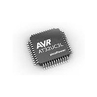
AT32UC3L032-D3UR Atmel, AT32UC3L032-D3UR Datasheet - Page 85

AT32UC3L032-D3UR
Manufacturer Part Number
AT32UC3L032-D3UR
Description
MCU AVR32 32KB FLASH 48TLLGA
Manufacturer
Atmel
Series
AVR®32 UC3r
Datasheet
1.AT32UC3L-EK.pdf
(858 pages)
Specifications of AT32UC3L032-D3UR
Core Processor
AVR
Core Size
32-Bit
Speed
50MHz
Connectivity
I²C, SPI, UART/USART
Peripherals
Brown-out Detect/Reset, DMA, PWM, WDT
Number Of I /o
36
Program Memory Size
32KB (32K x 8)
Program Memory Type
FLASH
Ram Size
16K x 8
Voltage - Supply (vcc/vdd)
1.62 V ~ 3.6 V
Data Converters
A/D 9x10b
Oscillator Type
Internal
Operating Temperature
-40°C ~ 85°C
Package / Case
48-TLLGA
Processor Series
AT32UC3x
Core
AVR32
Data Bus Width
32 bit
Data Ram Size
16 KB
Interface Type
SPI, TWI, USART
Maximum Clock Frequency
50 MHz
Number Of Programmable I/os
36
Number Of Timers
7
Maximum Operating Temperature
+ 85 C
Mounting Style
SMD/SMT
3rd Party Development Tools
EWAVR32, EWAVR32-BL
Development Tools By Supplier
AT32UC3L-EK
Minimum Operating Temperature
- 40 C
On-chip Adc
10 bit, 9 Channel
Lead Free Status / RoHS Status
Lead free / RoHS Compliant
Eeprom Size
-
Lead Free Status / Rohs Status
Details
- Current page: 85 of 858
- Download datasheet (13Mb)
8.5.3
8.6
32099F–11/2010
General-purpose Fuse Bits
Region Lock Bits
flash memory locations, the general-purpose fuse bits, and the security bit are erased (reset to
0xFF) after an Erase All.
The EA command also ensures that all volatile memories, such as register file and RAMs, are
erased before the security bit is erased.
Erase All operation is allowed only if no regions are locked, and the BOOTPROT fuses are con-
figured with a BOOTPROT region size of 0. Thus, if at least one region is locked, the bit LOCKE
in FSR is set and the command is cancelled. If the LOCKE bit in FCR is one, an interrupt request
is set generated.
When the command is complete, the FRDY bit in the Flash Status Register (FSR) is set. If an
interrupt has been enabled by writing FCR.FRDY to one, an interrupt request is generated. Two
errors can be detected in the FSR register after issuing the command:
The flash memory has p pages, and these pages are grouped into 16 lock regions, each region
containing p/16 pages. Each region has a dedicated lock bit preventing writing and erasing
pages in the region. After production, the device may have some regions locked. These locked
regions are reserved for a boot or default application. Locked regions can be unlocked to be
erased and then programmed with another application or other data.
To lock or unlock a region, the commands Lock Region Containing Page (LP) and Unlock
Region Containing Page (UP) are provided. Writing one of these commands, together with the
number of the page whose region should be locked/unlocked, performs the desired operation.
One error can be detected in the FSR register after issuing the command:
The lock bits are implemented using the lowest 16 general-purpose fuse bits. This means that
lock bits can also be set/cleared using the commands for writing/erasing general-purpose fuse
bits, see
is unlocked.
The lowermost pages in the flash can additionally be protected by the BOOTPROT fuses, see
Section
The flash memory has a number of general-purpose fuse bits that the application programmer
can use freely. The fuse bits can be written and erased using dedicated commands, and read
• Programming Error: A bad keyword and/or an invalid command have been written in the
• Lock Error: At least one lock region is protected, or BOOTPROT is different from 0. The erase
• Programming Error: A bad keyword and/or an invalid command have been written in the
FCMD register.
command has been aborted and no page has been erased. A “Unlock region containing
given page” (UP) command must be executed to unlock any locked regions.
FCMD register.
8.6.
Section
8.6. The general-purpose bit being in an erased (1) state means that the region
AT32UC3L016/32/64
85
Related parts for AT32UC3L032-D3UR
Image
Part Number
Description
Manufacturer
Datasheet
Request
R

Part Number:
Description:
KIT DEV/EVAL FOR AT32UC3L0
Manufacturer:
Atmel
Datasheet:

Part Number:
Description:
DEV KIT FOR AVR/AVR32
Manufacturer:
Atmel
Datasheet:

Part Number:
Description:
INTERVAL AND WIPE/WASH WIPER CONTROL IC WITH DELAY
Manufacturer:
ATMEL Corporation
Datasheet:

Part Number:
Description:
Low-Voltage Voice-Switched IC for Hands-Free Operation
Manufacturer:
ATMEL Corporation
Datasheet:

Part Number:
Description:
MONOLITHIC INTEGRATED FEATUREPHONE CIRCUIT
Manufacturer:
ATMEL Corporation
Datasheet:

Part Number:
Description:
AM-FM Receiver IC U4255BM-M
Manufacturer:
ATMEL Corporation
Datasheet:

Part Number:
Description:
Monolithic Integrated Feature Phone Circuit
Manufacturer:
ATMEL Corporation
Datasheet:

Part Number:
Description:
Multistandard Video-IF and Quasi Parallel Sound Processing
Manufacturer:
ATMEL Corporation
Datasheet:

Part Number:
Description:
High-performance EE PLD
Manufacturer:
ATMEL Corporation
Datasheet:

Part Number:
Description:
8-bit Flash Microcontroller
Manufacturer:
ATMEL Corporation
Datasheet:

Part Number:
Description:
2-Wire Serial EEPROM
Manufacturer:
ATMEL Corporation
Datasheet:


