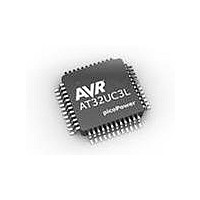
AT32UC3L032-D3UR Atmel, AT32UC3L032-D3UR Datasheet - Page 537

AT32UC3L032-D3UR
Manufacturer Part Number
AT32UC3L032-D3UR
Description
MCU AVR32 32KB FLASH 48TLLGA
Manufacturer
Atmel
Series
AVR®32 UC3r
Datasheet
1.AT32UC3L-EK.pdf
(858 pages)
Specifications of AT32UC3L032-D3UR
Core Processor
AVR
Core Size
32-Bit
Speed
50MHz
Connectivity
I²C, SPI, UART/USART
Peripherals
Brown-out Detect/Reset, DMA, PWM, WDT
Number Of I /o
36
Program Memory Size
32KB (32K x 8)
Program Memory Type
FLASH
Ram Size
16K x 8
Voltage - Supply (vcc/vdd)
1.62 V ~ 3.6 V
Data Converters
A/D 9x10b
Oscillator Type
Internal
Operating Temperature
-40°C ~ 85°C
Package / Case
48-TLLGA
Processor Series
AT32UC3x
Core
AVR32
Data Bus Width
32 bit
Data Ram Size
16 KB
Interface Type
SPI, TWI, USART
Maximum Clock Frequency
50 MHz
Number Of Programmable I/os
36
Number Of Timers
7
Maximum Operating Temperature
+ 85 C
Mounting Style
SMD/SMT
3rd Party Development Tools
EWAVR32, EWAVR32-BL
Development Tools By Supplier
AT32UC3L-EK
Minimum Operating Temperature
- 40 C
On-chip Adc
10 bit, 9 Channel
Lead Free Status / RoHS Status
Lead free / RoHS Compliant
Eeprom Size
-
Lead Free Status / Rohs Status
Details
- Current page: 537 of 858
- Download datasheet (13Mb)
23.6.8
23.6.9
23.6.9.1
23.6.9.2
32099F–11/2010
Interrupts
Peripheral Events
Input Peripheral Events
Output Peripheral Event
Note that the duty cycle registers will not be updated with the new values until the timebase
counter reaches its top value, in order to avoid glitches. The BUSY bit in SR will always be set
during this updating and synchronization period.
When the timebase counter overflows, the Timebase Overflow bit in the Status Register
(SR.TOFL) is set. If the corresponding bit in the Interrupt Mask Register (IMR) is set, an interrupt
request will be generated.
Since the user needs to wait until the user interface is available between each write due to syn-
chronization, a READY bit is provided in SR, which can be used to generate an interrupt
request.
The interrupt request will be generated if the corresponding bit in IMR is set. Bits in IMR are set
by writing a one to the corresponding bit in the Interrupt Enable Register (IER), and cleared by
writing a one to the corresponding bit in the Interrupt Disable Register (IDR). The interrupt
request remains active until the corresponding bit in SR is cleared by writing a one to the corre-
sponding bit in the Status Clear Register (SCR).
The pre-defined channels support input peripheral events from the Peripheral Event System. An
increase event (event_incr) will increase the duty cycle value by one, and a decrease event
(event_decr) will decrease the duty cycle value by one. If an increase event and a decrease
event occur at the same time, the duty cycle value will not be changed.
The number of channels supporting input peripheral events is device specific. Please refer to the
Module Configuration section at the end of this chapter for details.
Input peripheral events must be enabled by writing a one to the corresponding bit in the Chanel
Event Enable Register (CHEERm) before peripheral events can be used to control the duty
cycle value. Each bit in the register corresponds to one channel, where bit 0 corresponds to
channel 0 and so on. Both the increase and decrease events are enabled for the corresponding
channel when a bit in the CHEERm register is written to one.
The PWMA also supports one output peripheral event (event_ch0) to the Peripheral Event Sys-
tem. This output peripheral event is connected to channel 0 and will be asserted when the
timebase counter reaches the duty cycle value for channel 0. This output event is always
enabled.
AT32UC3L016/32/64
537
Related parts for AT32UC3L032-D3UR
Image
Part Number
Description
Manufacturer
Datasheet
Request
R

Part Number:
Description:
KIT DEV/EVAL FOR AT32UC3L0
Manufacturer:
Atmel
Datasheet:

Part Number:
Description:
DEV KIT FOR AVR/AVR32
Manufacturer:
Atmel
Datasheet:

Part Number:
Description:
INTERVAL AND WIPE/WASH WIPER CONTROL IC WITH DELAY
Manufacturer:
ATMEL Corporation
Datasheet:

Part Number:
Description:
Low-Voltage Voice-Switched IC for Hands-Free Operation
Manufacturer:
ATMEL Corporation
Datasheet:

Part Number:
Description:
MONOLITHIC INTEGRATED FEATUREPHONE CIRCUIT
Manufacturer:
ATMEL Corporation
Datasheet:

Part Number:
Description:
AM-FM Receiver IC U4255BM-M
Manufacturer:
ATMEL Corporation
Datasheet:

Part Number:
Description:
Monolithic Integrated Feature Phone Circuit
Manufacturer:
ATMEL Corporation
Datasheet:

Part Number:
Description:
Multistandard Video-IF and Quasi Parallel Sound Processing
Manufacturer:
ATMEL Corporation
Datasheet:

Part Number:
Description:
High-performance EE PLD
Manufacturer:
ATMEL Corporation
Datasheet:

Part Number:
Description:
8-bit Flash Microcontroller
Manufacturer:
ATMEL Corporation
Datasheet:

Part Number:
Description:
2-Wire Serial EEPROM
Manufacturer:
ATMEL Corporation
Datasheet:


