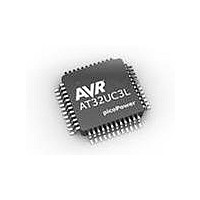
AT32UC3L032-D3UR Atmel, AT32UC3L032-D3UR Datasheet - Page 744

AT32UC3L032-D3UR
Manufacturer Part Number
AT32UC3L032-D3UR
Description
MCU AVR32 32KB FLASH 48TLLGA
Manufacturer
Atmel
Series
AVR®32 UC3r
Datasheet
1.AT32UC3L-EK.pdf
(858 pages)
Specifications of AT32UC3L032-D3UR
Core Processor
AVR
Core Size
32-Bit
Speed
50MHz
Connectivity
I²C, SPI, UART/USART
Peripherals
Brown-out Detect/Reset, DMA, PWM, WDT
Number Of I /o
36
Program Memory Size
32KB (32K x 8)
Program Memory Type
FLASH
Ram Size
16K x 8
Voltage - Supply (vcc/vdd)
1.62 V ~ 3.6 V
Data Converters
A/D 9x10b
Oscillator Type
Internal
Operating Temperature
-40°C ~ 85°C
Package / Case
48-TLLGA
Processor Series
AT32UC3x
Core
AVR32
Data Bus Width
32 bit
Data Ram Size
16 KB
Interface Type
SPI, TWI, USART
Maximum Clock Frequency
50 MHz
Number Of Programmable I/os
36
Number Of Timers
7
Maximum Operating Temperature
+ 85 C
Mounting Style
SMD/SMT
3rd Party Development Tools
EWAVR32, EWAVR32-BL
Development Tools By Supplier
AT32UC3L-EK
Minimum Operating Temperature
- 40 C
On-chip Adc
10 bit, 9 Channel
Lead Free Status / RoHS Status
Lead free / RoHS Compliant
Eeprom Size
-
Lead Free Status / Rohs Status
Details
- Current page: 744 of 858
- Download datasheet (13Mb)
31.4.7
31.4.8
31.4.9
31.4.9.1
Figure 31-7. Scanning in JTAG Instruction
31.4.9.2
32099F–11/2010
TCK
TAP State
TMS
TDI
TDO
How to Initialize the Module
How to disable the module
Typical Sequence
Scanning in JTAG Instruction
Scanning in/out Data
TLR
To enable the JTAG pins the TCK pin must be held low while the RESET_N pin is released.
After enabling the JTAG interface the halt bit is set automatically to prevent the system from run-
ning code after the interface is enabled. To make the CPU run again set halt to zero using the
HALT command..
JTAG operation when RESET_N is pulled low is not possible.
Independent of the initial state of the TAP Controller, the Test-Logic-Reset state can always be
entered by holding TMS high for 5 TCK clock periods. This sequence should always be applied
at the start of a JTAG session and after enabling the JTAG pins to bring the TAP Controller into
a defined state before applying JTAG commands. Applying a 0 on TMS for 1 TCK period brings
the TAP Controller to the Run-Test/Idle state, which is the starting point for JTAG operations.
To disable the JTAG pins the TCK pin must be held high while RESET_N pin is released.
Assuming Run-Test/Idle is the present state, a typical scenario for using the JTAG Interface
follows.
At the TMS input, apply the sequence 1, 1, 0, 0 at the rising edges of TCK to enter the Shift
Instruction Register (Shift-IR) state. While in this state, shift the 5 bits of the JTAG instructions
into the JTAG instruction register from the TDI input at the rising edge of TCK. During shifting,
the JTAG outputs status bits on TDO, refer to
input must be held low during input of the 4 LSBs in order to remain in the Shift-IR state. The
JTAG Instruction selects a particular Data Register as path between TDI and TDO and controls
the circuitry surrounding the selected Data Register.
Apply the TMS sequence 1, 1, 0 to re-enter the Run-Test/Idle state. The instruction is latched
onto the parallel output from the shift register path in the Update-IR state. The Exit-IR, Pause-IR,
and Exit2-IR states are only used for navigating the state machine.
At the TMS input, apply the sequence 1, 0, 0 at the rising edges of TCK to enter the Shift Data
Register (Shift-DR) state. While in this state, upload the selected Data Register (selected by the
present JTAG instruction in the JTAG Instruction Register) from the TDI input at the rising edge
RTI SelDR SelIR CapIR ShIR
Instruction
Section 31.5
ImplDefined
AT32UC3L016/32/64
for a description of these. The TMS
Ex1IR UpdIR RTI
744
Related parts for AT32UC3L032-D3UR
Image
Part Number
Description
Manufacturer
Datasheet
Request
R

Part Number:
Description:
KIT DEV/EVAL FOR AT32UC3L0
Manufacturer:
Atmel
Datasheet:

Part Number:
Description:
DEV KIT FOR AVR/AVR32
Manufacturer:
Atmel
Datasheet:

Part Number:
Description:
INTERVAL AND WIPE/WASH WIPER CONTROL IC WITH DELAY
Manufacturer:
ATMEL Corporation
Datasheet:

Part Number:
Description:
Low-Voltage Voice-Switched IC for Hands-Free Operation
Manufacturer:
ATMEL Corporation
Datasheet:

Part Number:
Description:
MONOLITHIC INTEGRATED FEATUREPHONE CIRCUIT
Manufacturer:
ATMEL Corporation
Datasheet:

Part Number:
Description:
AM-FM Receiver IC U4255BM-M
Manufacturer:
ATMEL Corporation
Datasheet:

Part Number:
Description:
Monolithic Integrated Feature Phone Circuit
Manufacturer:
ATMEL Corporation
Datasheet:

Part Number:
Description:
Multistandard Video-IF and Quasi Parallel Sound Processing
Manufacturer:
ATMEL Corporation
Datasheet:

Part Number:
Description:
High-performance EE PLD
Manufacturer:
ATMEL Corporation
Datasheet:

Part Number:
Description:
8-bit Flash Microcontroller
Manufacturer:
ATMEL Corporation
Datasheet:

Part Number:
Description:
2-Wire Serial EEPROM
Manufacturer:
ATMEL Corporation
Datasheet:


